Semiconductor memory device

a memory device and semiconductor technology, applied in the direction of semiconductor devices, electrical devices, transistors, etc., can solve the problems of inapplicability of floating gate memory, inability to solve the fundamental problem of lifetime, and the use of such a method does not solve the fundamental problem of life, so as to achieve the degree of integration of the memory cell array and achieve the effect of high degree of integration

Active Publication Date: 2013-09-05
SEMICON ENERGY LAB CO LTD
View PDF2 Cites 26 Cited by
  • Summary
  • Abstract
  • Description
  • Claims
  • Application Information

AI Technical Summary

Benefits of technology

[0015]In a semiconductor memory device of one embodiment of the present invention, a memory cell includes two transistors and one capacitor which are arranged three-dimensionally. By three-dimensionally arranging the transistors and the capacitor, which are included in the memory cell, the cell density per unit area of a memory cell array is increased. One of the transistors provided in the memory cell is a transistor for controlling the amount of electric charge of the capacitor. In one embodiment of the present invention, the leakage current of this transistor is reduced. To reduce the leakage current of the transistor, a semiconductor material having a wider band gap than silicon is used for a channel region. Accordingly, a semiconductor memory device which can hold stored data for a certain period even when power is not supplied is provided.
[0036]According to one embodiment of the present invention, by placing the second semiconductor layer of the second transistor so as to overlap with the first gate electrode, the degree of integration of the memory cell array can be improved. Further, by forming the transistor for controlling the amount of electric charge of the capacitor in the memory cell using a semiconductor material having a wider band gap than silicon, a semiconductor memory device which can hold stored data even when power is not supplied can be provided. Further, by forming the transistor for controlling the amount of electric charge of the capacitor in the memory cell using a transistor having a smaller leakage current, a semiconductor memory device which is non-volatile and does not have a limitation on the number of write cycles can be provided.

Problems solved by technology

However, a gate insulating layer included in a memory element deteriorates by tunneling current generated in writing, so that the memory element stops its function after a predetermined number of writing operations.
However, a complex peripheral circuit is needed to realize this method.
Moreover, employing such a method does not solve the fundamental problem of lifetime.
In other words, a floating gate memory is not suitable for applications in which data is frequently rewritten.
Thus, the semiconductor memory device can hold data for a long period.

Method used


Image

  • Semiconductor memory device
  • Semiconductor memory device
  • Semiconductor memory device

Examples


embodiment 1

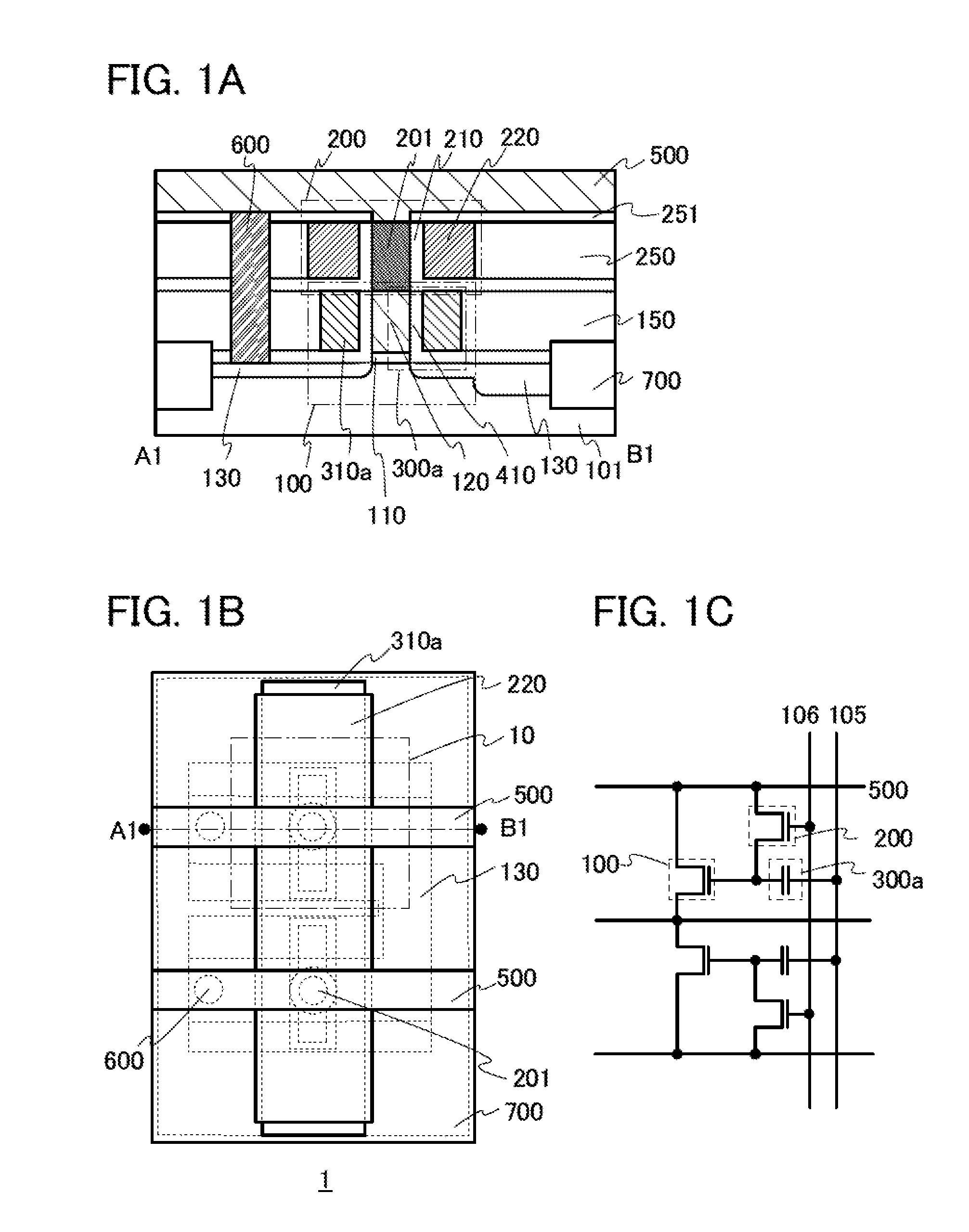
[0057]In this embodiment, an example of a structure of a semiconductor memory device, which is one embodiment of the present invention, is described with reference to FIGS. 1A to 1C.

[0058]FIG. 1B is a schematic top view of a semiconductor memory device 1, and FIG. 1A is a schematic cross-sectional view along dashed dotted line A1-B1 in FIG. 1B. FIG. 1C is a circuit diagram of the semiconductor memory device 1.

[0059]The semiconductor memory device 1 described in this embodiment includes a plurality of bit lines 500 which are parallel to each other, and a plurality of first word lines 105 and a plurality of second word lines 106 which are perpendicular to the bit lines 500. Further, a first transistor 100, a second transistor 200, and a capacitor 300a are formed in a region overlapping with the bit line 500, the first word line 105, and the second word line 106. A memory cell 10 includes the first transistor 100, the second transistor 200, and the capacitor 300a. Note that the first w...

embodiment 2

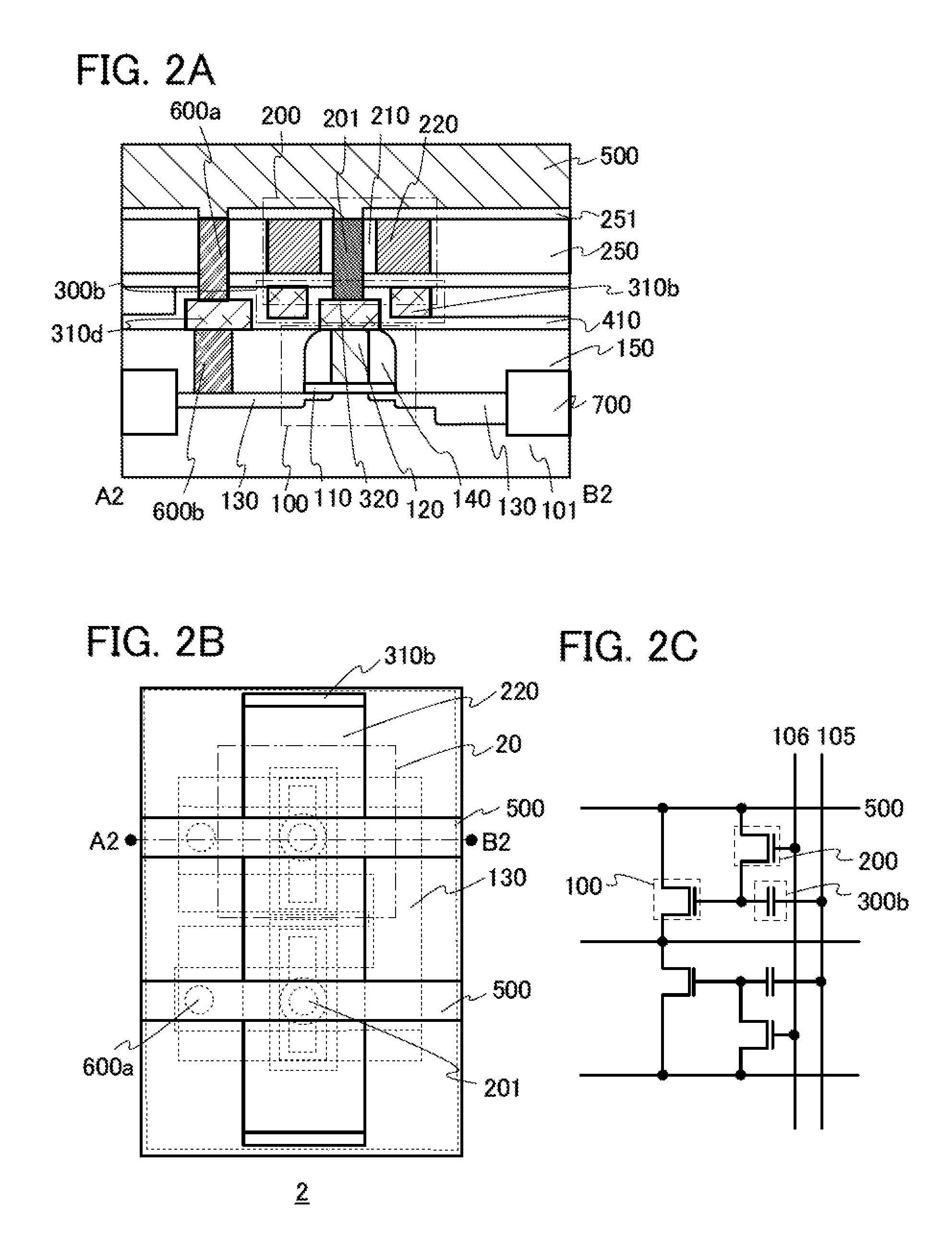
[0101]In this embodiment, an example of a structure of a semiconductor memory device, which is one embodiment of the present invention, is described with reference to FIGS. 2A to 2C.

[0102]FIG. 2B is a schematic top view of a semiconductor memory device 2, and FIG. 2A is a schematic cross-sectional view along dashed dotted line A2-B2 in FIG. 2B. FIG. 2C is a circuit diagram of the semiconductor memory device 2.

[0103]The semiconductor memory device 2 described in this embodiment includes the plurality of bit lines 500 which are parallel to each other and the plurality of first word lines 105 and the plurality of second word lines 106 which are perpendicular to the bit lines 500. Further, the first transistor 100, the second transistor 200, and a capacitor 300b are formed in a region overlapping with the bit line 500, the first word line 105, and the second word line 106. A memory cell 20 includes the first transistor 100, the second transistor 200, and the capacitor 300b. Note that th...

embodiment 3

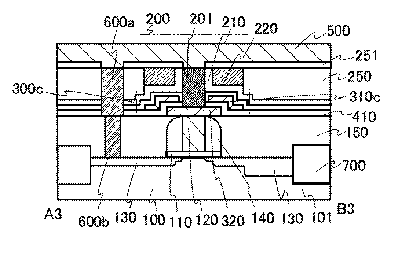
[0120]In this embodiment, an example of a structure of a semiconductor memory device, which is one embodiment of the present invention, is described with reference to FIGS. 3A to 3C.

[0121]FIG. 3B is a schematic top view of a semiconductor memory device 3, and FIG. 3A is a schematic cross-sectional view along dashed dotted line A3-B3 in FIG. 3B. FIG. 3C is a circuit diagram of the semiconductor memory device 3.

[0122]The semiconductor memory device 3 described in this embodiment includes the plurality of bit lines 500 which are parallel to each other and the plurality of first word lines 105 and the plurality of second word lines 106 which are perpendicular to the bit lines 500. Further, the first transistor 100, the second transistor 200, and a capacitor 300c are formed in a region overlapping with the bit line 500, the first word line 105, and the second word line 106. A memory cell 30 includes the first transistor 100, the second transistor 200, and the capacitor 300c. Note that th...


PUM


Abstract

To provide a highly integrated semiconductor memory device. To provide a semiconductor memory device which can hold stored data even when power is not supplied. To provide a semiconductor memory device which has a large number of write cycles. The degree of integration of a memory cell array is increased by forming a memory cell including two transistors and one capacitor which are arranged three-dimensionally. The electric charge accumulated in the capacitor is prevented from being leaking by forming a transistor for controlling the amount of electric charge of the capacitor in the memory cell using a wide-gap semiconductor having a wider band gap than silicon. Accordingly, a semiconductor memory device which can hold stored data even when power is not supplied can be provided.

Description

BACKGROUND OF THE INVENTION[0001]1. Field of the Invention[0002]The present invention relates to a semiconductor memory device.[0003]2. Description of the Related Art[0004]As semiconductor memory devices are integrated, a need for reduction of the area occupied by semiconductor elements arises. For example, in order to increase the degree of integration of a transistor, which is one of semiconductor elements, a so-called vertical transistor in which a channel is formed vertically to a substrate is known. When this structure is applied, a source electrode or a drain electrode overlaps with an active layer in which a channel is formed, so that the area occupied by the transistor can be reduced (for example, see Patent Document 1). As a result, a semiconductor memory device including such transistors can be integrated.[0005]Semiconductor memory devices are classified into volatile semiconductor memory devices that lose stored data when power supply stops, and non-volatile semiconductor...

Claims


Application Information

Patent Timeline
Patent Type & Authority Applications(United States)
IPC IPC(8): H01L27/108
CPCH01L27/108H01L27/10832H01L27/10835H01L27/1156H10B12/00H10B41/70H01L29/7869H01L29/66742H01L29/78696H01L29/42392H10B12/373H10B12/377H10B99/00
Inventor ARAI, YASUYUKI
Owner SEMICON ENERGY LAB CO LTD
Why Eureka
Try Eureka