Gallium-nitride based multi-quantum well light-emitting diode n-type contact layer structure

a gallium-nitride and multi-quantum well technology, applied in the field of gallium-nitride based multi-quantum well light-emitting diodes, can solve the problems of n-type gan contact layer easily chapped and snapped, affecting the epitaxial quality of gan-based mqw, and excessive stress to develop and accumulate. , to achieve the effect of convenient formation

Active Publication Date: 2006-04-20
LUMENS +1
View PDF2 Cites 24 Cited by
  • Summary
  • Abstract
  • Description
  • Claims
  • Application Information

AI Technical Summary

Benefits of technology

[0009] The present invention provides an epitaxial structure for the GaN-based MQW LEDs' n-type GaN contact layers, so that the limitations and disadvantages from the prior arts can be obviated practically.
[0010] The theory behind the present invention would be apparent from a study of the attached FIG. 1. FIG. 1 is a graph showing group III nitrides in a coordinate system of lattice constant and band gap. As shown in FIG. 1, GaN has a lattice constant a0 around 3.18 Å. Extended from GaN's position inFIG. 1 vertically along a lattice matching line, it can be seen that aluminum-indium-gallium-nitride (AlxInyGa1-x-yN, 0≦x, y<1, x+y≦1) has an identical lattice constant to but has a wider band gap than that of GaN. Then, instead of using Si-doped GaN, an n-type contact layer having high doping density (>1×1019 cm3) and low resistivity can be achieved through a superlattice structure combining two types of material, AlmInnGa1-m-nN and AlpInqGa1-p-qN (0≦m, n<1, 0<p, q<1, p+q≦1, m<p), each having its specific composition and doping density. In addition, by controlling the composition of Al, In, and Ga in the two materials, the n-type contact layer would have a compatible lattice constant with the substrate and the epitaxial structure of the GaN-based MQW LEDs. This n-type contact layer would not chap from the heavy Si doping, have a superior quality, and reduce the difficulties of forming n-type ohmic contact electrode. In turn, the GaN-based MQW LEDs would require a lower operation voltage.

Problems solved by technology

However, it is observed that, during practical fabricating processes, the n-type GaN contact layer would be easily chapped and snapped, as the heavy Si doping causes incompatible lattice constants among the epitaxial layers of the GaN-based MQW LEDs, that, in turn, causes excessive stress to develop and accumulate.
These undesirable results not only affect the epitaxial quality of the GaN-based MQW LEDs, but also add additional difficulties in the formation of the n-type ohmic contact electrode on top of the n-type GaN contact layer.
In summary, these shortcomings would result in an inferior electrical characteristics or conductivity in the GaN-based MQW LEDs.
In the worst case, the GaN-based MQW LEDs would be un-useable.
Therefore, the GaN-based MQW LEDs containing this type of conventional n-type GaN contact layers, on one hand, require a higher operation voltage and, thereby, consume more powers.
On the other hand, the GaN-based MQW LEDs would have a low yield rate, causing the production cost to rise.
Additionally, pin holes are easier to form in the heavily Si-doped n-type GaN contact layer, causing the semiconducting characteristics of the GaN-based MQW LEDs to deteriorate.
Current leakage is also possible during the operation of the GaN-based MQW LEDs.

Method used


Image

  • Gallium-nitride based multi-quantum well light-emitting diode n-type contact layer structure
  • Gallium-nitride based multi-quantum well light-emitting diode n-type contact layer structure
  • Gallium-nitride based multi-quantum well light-emitting diode n-type contact layer structure

Examples


first embodiment

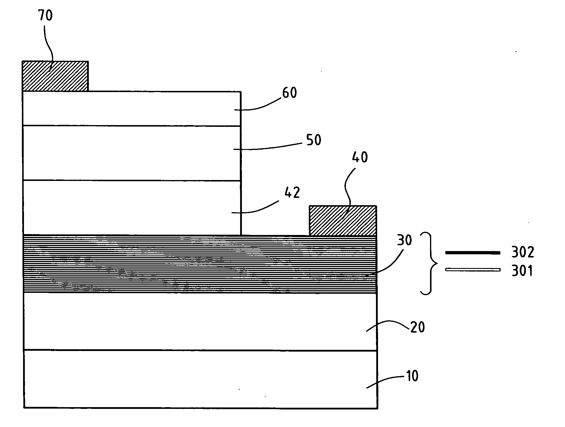
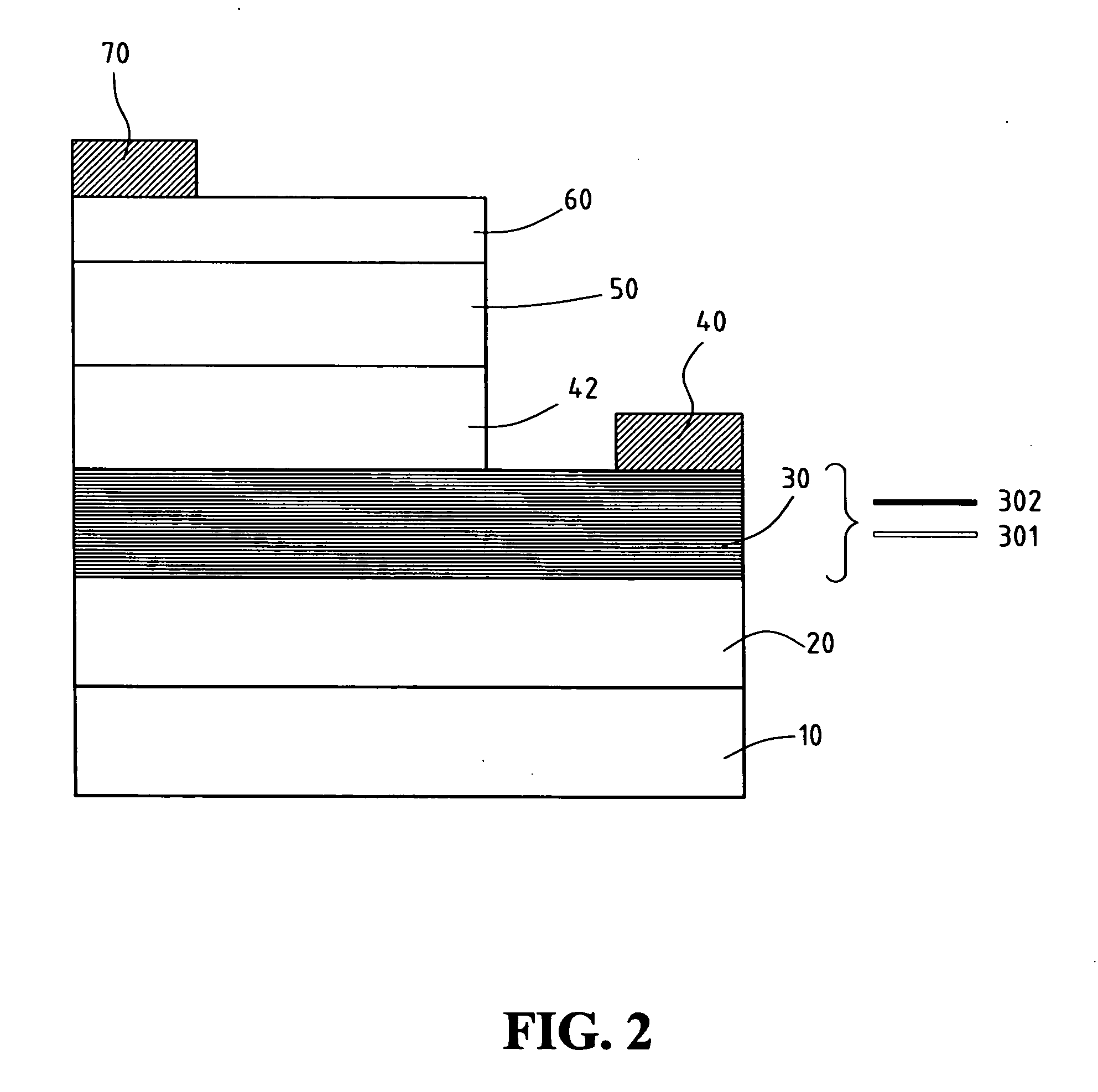
[0018]FIG. 2 is a schematic diagram showing the epitaxial structure of the GaN-based MQW LED according to the present invention. As shown in FIG. 2, the GaN-based LED has a substrate 10 made of C-plane, R-plane, or A-plane aluminum-oxide monocrystalline (sapphire), or an oxide monocrystalline having a lattice constant compatible with that of nitride semiconductors. The substrate 10 can also be made of SiC (6H—SiC or 4H—SiC), Si, ZnO, GaAs, or MgAl2O4. Generally, the most common material used for the substrate 10 is sapphire or SiC. A buffer layer 20 made of AlaGabIn1-a-bN (0≦a, b10. On top of the buffer layer 20, an n-type contact layer 30 is formed, which is the major focus of the present invention. Then, on top of n-type contact layer 30, an active layer 42 made of InGaN covers a part of the n-type contact layer 30's upper surface. A negative electrode 40, on the other hand, is on top of another part of the n-type contact layer 30's upper surface not covered by the active layer 42...

fourth embodiment

[0023]FIG. 5 is a schematic diagram showing the epitaxial structure of the GaN-based MQW LED according to the present invention. As shown in FIG. 5, the n-type contact layer 36 has a structure identical to those of the n-type contact layers of the previous embodiments. The only difference lies in the materials used for the n-type contact layer 36. Within this embodiment of the present invention, as shown in FIG. 5, the n-type contact layer 36 has a superlattice structure formed by multiple Si-doped AlInGaN base layers 361 and multiple Si-doped AlInGaN base layers 362, alternately stacked on top of each other. Among them, the AlInGaN base layers 362 have wider band gaps than those of the AlInGaN base layers 361. The n-type contact layer 36 can have either an AlInGaN base layers 361 or an AlInGaN base layers 362 as the bottommost base layer. That is, the n-type contact layer 36 can comprise an AlInGaN base layer 361, an AlInGaN base layer 362, another AlInGaN base layer 361, etc., seq...


PUM


Abstract

A structure for the n-type contact layer in the GaN-based MQW LEDs is provided. Instead of using Si-doped GaN as commonly found in conventional GaN-based MQW LEDs, the n-type contact layer provided by the present invention achieves high doping density (>1×1019 cm−3) and low resistivity through a superlattice structure combining two types of materials, AlmInnGa1-m-nN and AlpInqGa1-p-qN (0≦m, n<1, 0<p, q<1, p+q≦1, m<p), each having its specific composition and doping density. In addition, by controlling the composition of Al, In, and Ga in the two materials, the n-type contact layer would have a compatible lattice constant with the substrate and the epitaxial structure of the GaN-based MQW LEDs. This n-type contact layer, therefore, would not chap from the heavy Si doping, have a superior quality, and reduce the difficulties of forming n-type ohmic contact electrode. In turn, the GaN-based MQW LEDs would require a lower operation voltage.

Description

BACKGROUND OF THE INVENTION [0001] 1. Field of the Invention [0002] The present invention generally relates to the gallium-nitride based multi-quantum well light-emitting diodes and, more particularly, to the n-type contact layer structure of the gallium-nitride based multi-quantum well light-emitting diodes. [0003] 2. The Prior Arts [0004] Gallium-nitride (GaN) materials can achieve a wide range of band gaps by controlling the GaN-based materials' compositions. As such, various colored light-emitting diodes (LEDs), especially those blue or purple light LEDs that require wide band gaps, can be produced using GaN-based materials. These GaN-based LEDs therefore have been the research and development focus in recent years. [0005] Within conventional GaN-based LEDs, the active layers usually adopt a multi-quantum well (MQW) structure with GaN and indium-gallium-nitride (InxGa1-xN, 0≦x≦1) as potential wells. Photons are then generated through the recombination of the electrons and holes ...

Claims


Application Information

Patent Timeline
Patent Type & Authority Applications(United States)
IPC IPC(8): H01L29/225
CPCB82Y20/00H01L21/0237H01L21/02458H01L21/02505H01L21/0254H01L21/02573H01L33/04H01L33/06H01L33/14H01L33/32
Inventor WU, LIANG-WENTU, RU-CHINYU, CHENG-TSANGWEN, TZU-CHICHIEN, FEN-REN
Owner LUMENS
Why Eureka
Try Eureka