Light emitting diode

a light-emitting diode and semiconductor technology, applied in the field of semiconductor light-emitting devices, can solve the problems of piezoelectric polarization charges, achieve the effects of enhancing the recombination of electrons, reducing the hole barrier, and increasing the electron barrier

Inactive Publication Date: 2010-07-29
ARMY US SEC THE THE
View PDF3 Cites 24 Cited by
  • Summary
  • Abstract
  • Description
  • Claims
  • Application Information

AI Technical Summary

Benefits of technology

[0015]A preferred embodiment of the present invention provides a new single heterojunction III-nitride design for LEDs and other light emitting crystal structures, with either p-down Ga-polar or p- up N-polar. A preferred embodiment of the present invention comprises a heterojunction structure without quantum wells. The spontaneous / piezoelectric polarization charge at the interface of the heterojunction is negative resulting in an increase in the electron barrier, substantially eliminates the hole barrier. A 2D hole-gas forms near the interface, which significantly enhances the recombination of electrons with holes. The present invention exhibits a higher current to light conversion efficiency than conventional devices. In addition, no electron blocking layer is required resulting in a lower turn on voltage, higher conversion efficiency, and longer device lifetime due to lower thermal load. The band gap is wider in the p-type layer so that the recombination occurs in the n-type layer. In one preferred embodiment, the negative polarization charge is obtained by utilization of p-type layer having a spontaneous polarization charge less than the n-type layer spontaneous polarization charge. In addition, lattice mismatching creates a piezoelectric polarization charge. The present invention is not limited to any particular material composition and a variety of polar semiconductor materials may be selected.

Problems solved by technology

In addition, lattice mismatching creates a piezoelectric polarization charge.

Method used


Image

  • Light emitting diode
  • Light emitting diode
  • Light emitting diode

Examples


Embodiment Construction

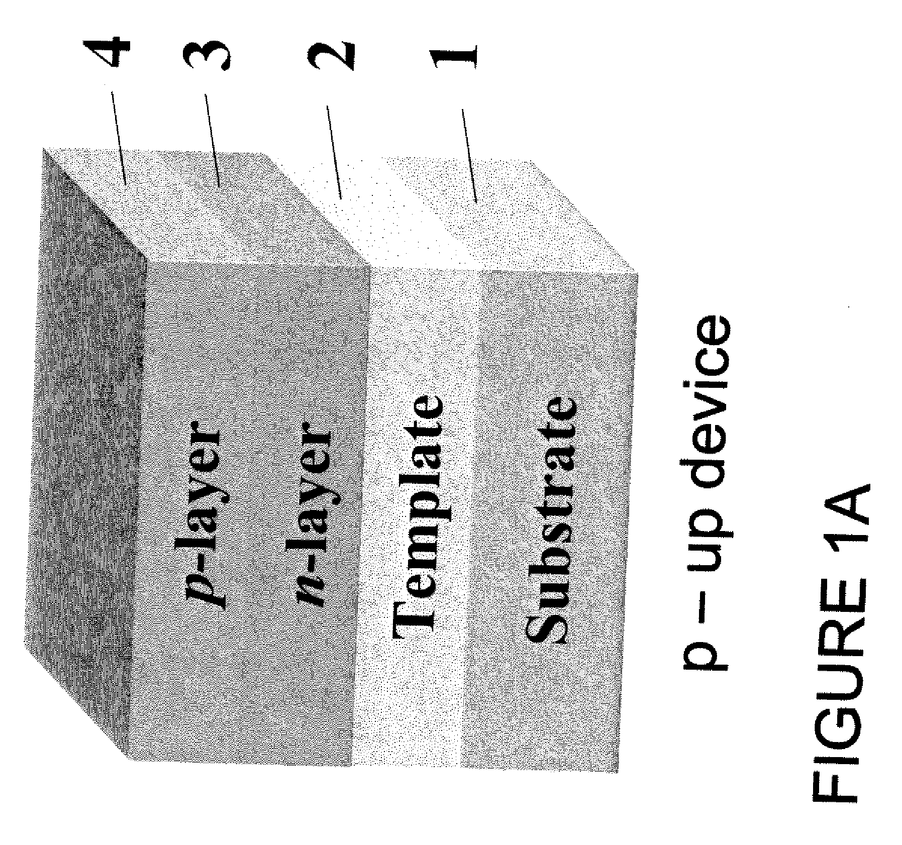
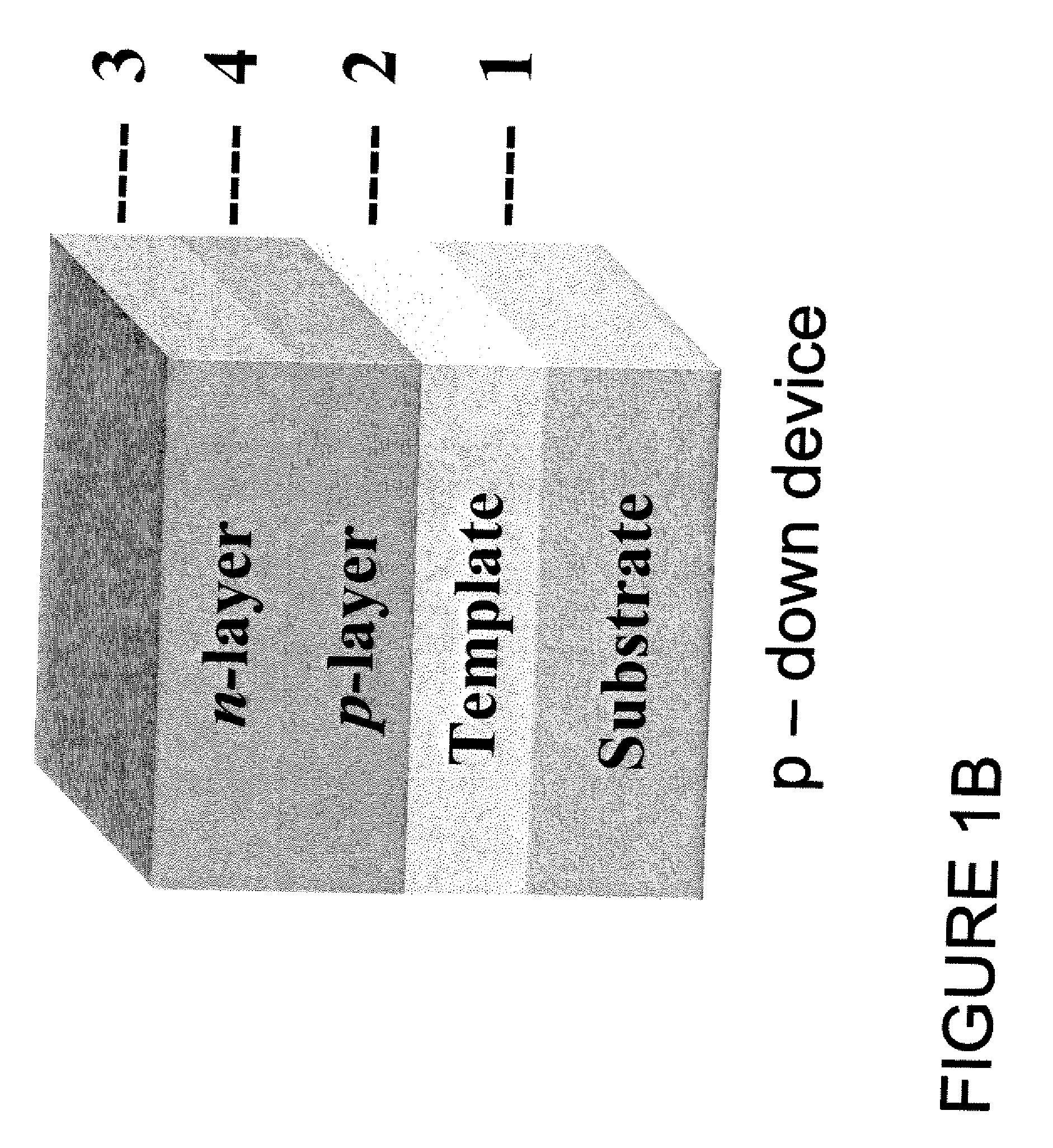
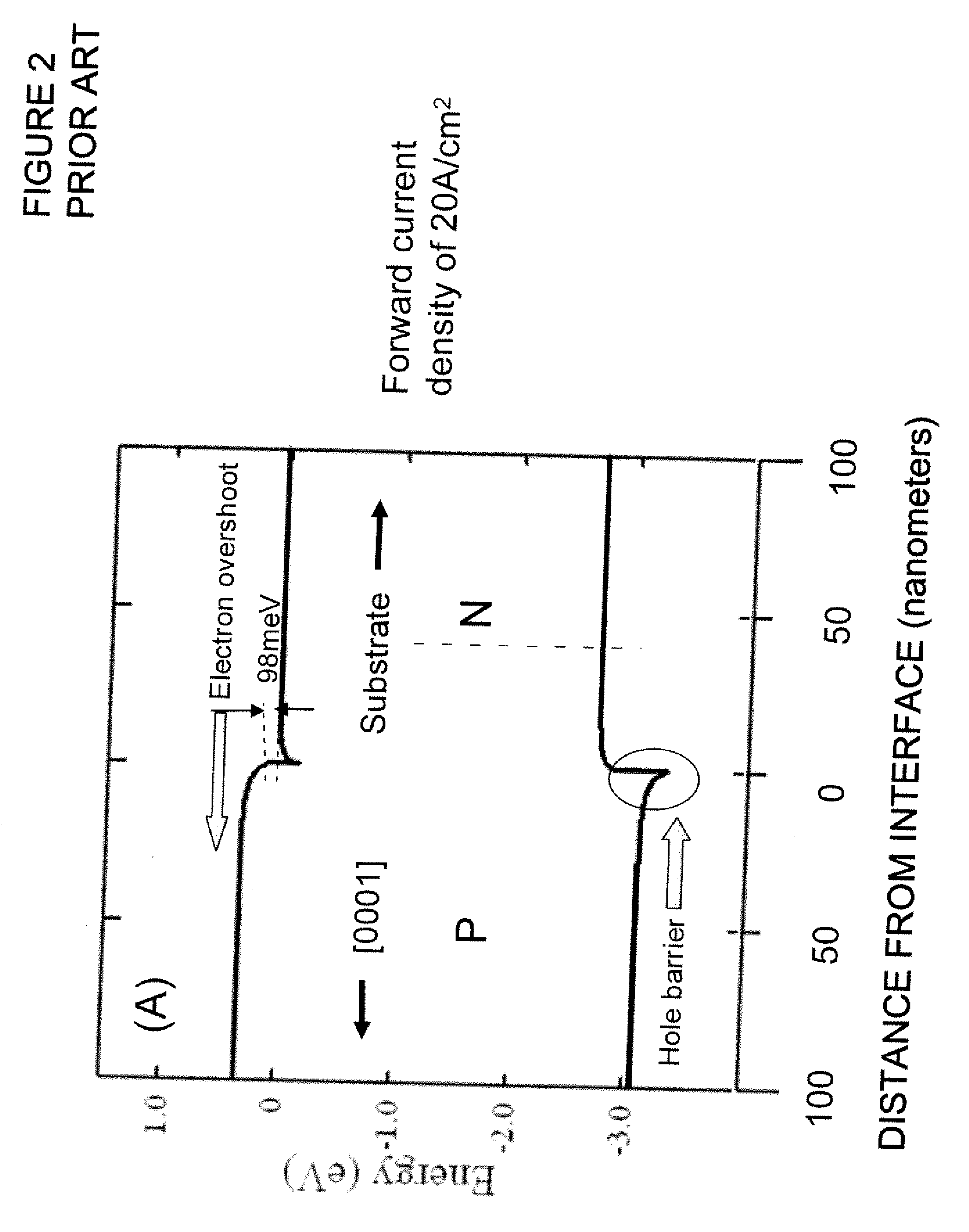
[0047]The embodiments of the invention and the various features and advantageous details thereof are explained more fully with reference to the non-limiting embodiments that are illustrated in the accompanying drawings and detailed in the following description. It should be noted that the features illustrated in the drawings are not necessarily drawn to scale. Descriptions of well-known components and processing techniques are omitted so as to not unnecessarily obscure the embodiments of the invention. The examples used herein are intended merely to facilitate an understanding of ways in which the embodiments of the invention may be practiced and to further enable those of skilled in the art to practice the embodiments of the invention. Accordingly, the examples should not be construed as limiting the scope of the embodiments of the invention.

[0048]The terminology used herein is for the purpose of describing particular embodiments only and is not intended to limit the full scope of ...


PUM


Abstract

In a preferred embodiment, a light emitting device comprising: a polar template; a p-type layer grown on the polar template; the p-type layer having a first polarization vector; the first polarization vector having a first projection relative to a growth direction; an n-type layer grown on the p-type layer; the n-type layer having a second polarization vector; the second polarization vector having a second projection relative to said growth direction that is larger than the first projection of the first polarization vector for the p-type layer; the n-type layer and p-type layer forming an interface; whereby the first polarization vector in the p-layer and second polarization vector in the n-layer create a discontinuity at the interface resulting in a negative charge appearing at the interface. In another preferred embodiment, a light emitting device comprising: a polar template; a n-type layer grown on the template; the n-type layer having a first polarization vector; the first polarization vector having a first projection relative to a growth direction; an p-type layer grown on the n-type layer; the p-type layer having a second polarization vector; the second polarization vector having a second projection relative to said growth direction that is larger than the first projection of the first polarization vector for the p-type layer; the n-type layer and p-type layer forming an interface; whereby the first polarization vector in the p-layer and second polarization vector in the n-layer create a discontinuity at the interface resulting in a negative charge appearing at the interface.

Description

CROSS-REFERENCE TO RELATED APPLICATIONS[0001]This application claims priority of U.S. Provisional Patent Application Ser. No. 61 / 051,219 filed May 7, 2008, which is incorporated herein by reference.GOVERNMENT INTEREST[0002]The invention described herein may be manufactured, used, and / or licensed by or for the United States Government.FIELD OF INVENTION[0003]The invention generally relates to semiconductor light emitters, and in particular, highly efficient III-nitride semiconductors for use in light emitting diodes (LEDs) and / or lasers.DESCRIPTION OF THE PRIOR ART[0004]A semiconductor's ability to conduct can be modified through the process of “doping” during the growth process. Growth of conventional semiconductor materials can be performed via a variety of different growth processes and is dependent upon the type of material being grown. These growth processes can include, but is not limited to: metal-organic chemical vapor deposition, molecular beam epitaxy, pulsed laser ablation...

Claims


Application Information

Patent Timeline
Patent Type & Authority Applications(United States)
IPC IPC(8): H01L33/00
CPCH01L33/32H01L33/18
Inventor REED, MEREDITH L.WRABACK, MICHAELSHEN, PAUL
Owner ARMY US SEC THE THE
Why Eureka
Try Eureka