Method of measuring thickness of thin layer in semiconductor device and apparatus for performing method

a thin layer and semiconductor technology, applied in semiconductor/solid-state device testing/measurement, instruments, material analysis, etc., can solve the problems of optical distortion, device failure, and cost and time-consuming methods

Active Publication Date: 2008-12-16
SAMSUNG ELECTRONICS CO LTD
View PDF8 Cites 2 Cited by
  • Summary
  • Abstract
  • Description
  • Claims
  • Application Information

AI Technical Summary

Problems solved by technology

Where the gate oxide layer is too thin, it may break down under normal operating conditions, corrupting the device.
Unfortunately, this method is both costly and time consuming, and as a result, researchers have developed other “non-destructive” techniques, i.e., techniques that do not require cutting up a wafer, for measuring the physical characteristics of a thin layer.
However, because layers formed beneath the thin layer can create optical distortion, e.g., in the form of interference, the optical techniques are generally not applied to a working wafer where a semiconductor device is formed.
Unfortunately, conventional optical technologies for measuring the physical characteristics of a thin layer still suffer from a variety of inaccuracies and inefficiencies.
For example, characteristics inferred from measurements performed on the monitoring wafer may not accurately reflect the true characteristics of the thin layer on the working wafer.
In addition, processes for forming a thin layer on the monitoring wafer increase the time and cost of manufacturing a semiconductor device.
Unfortunately, the GOF value may not accurately reflect the level of similarity between the measured signal spectrum and the theoretical spectrum.

Method used


Image

  • Method of measuring thickness of thin layer in semiconductor device and apparatus for performing method
  • Method of measuring thickness of thin layer in semiconductor device and apparatus for performing method
  • Method of measuring thickness of thin layer in semiconductor device and apparatus for performing method

Examples


Embodiment Construction

[0042]Exemplary embodiments of the invention are described below with reference to the corresponding drawings. These embodiments are presented as teaching examples. The actual scope of the invention is defined by the claims that follow.

[0043]In this written description, elements described as being “on,”“connected to,” or “coupled to” another element or layer can be directly on, connected or coupled to the other element or layer, or intervening elements or layers may be present. However, when an element is referred to as being “directly on,”“directly connected to,” or “directly coupled to” another element or layer, there are no intervening elements or layers present. The term “and / or” is used to refer to any or all combinations of one or more items in a list.

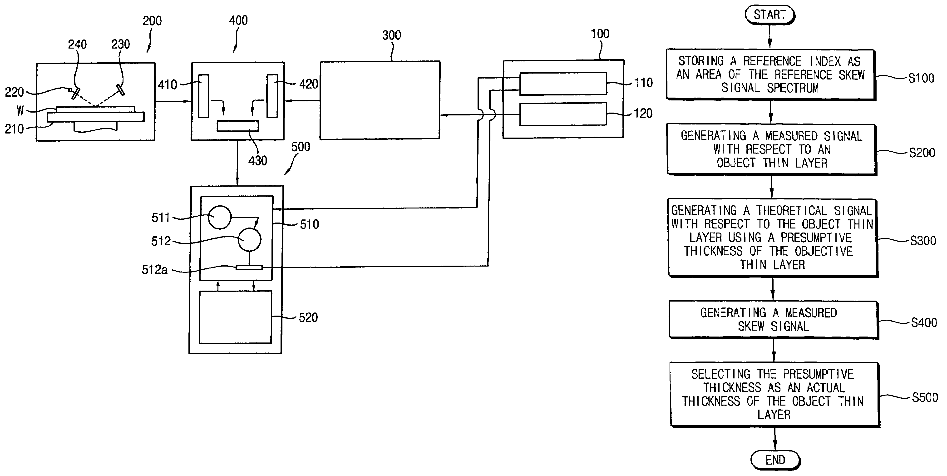
[0044]FIG. 4 is a schematic view illustrating an apparatus for measuring a thickness of a target thin layer formed on a substrate such as a wafer in accordance with an exemplary embodiment of the present invention. Referring to F...


PUM


Abstract

A method of measuring the thickness of a thin layer formed on a substrate comprises generating a measured signal spectrum by reflecting a light off of the thin layer and analyzing a resulting reflected light. The method further comprises generating a theoretical signal spectrum based on a putative thickness of the thin layer, and computing a skew signal spectrum as a difference between the measured signal spectrum and the theoretical spectrum. The method still comprises computing a reliability index by dividing a reference index by an area of the skew signal spectrum and using the reliability index to update the theoretical signal spectrum in a regression fitting process.

Description

BACKGROUND OF THE INVENTION[0001]1. Field of the Invention[0002]Embodiments of the present invention relate generally to a method of measuring the thickness of a thin layer in a semiconductor device, and an apparatus for performing the method. More particularly, embodiments of the invention relate to a method and apparatus for measuring the thickness of a thin layer using a regression fitting process.[0003]A claim of priority is made to Korean Patent Application No. 2005-65878, filed on Jul. 20, 2005, the disclosure of which is hereby incorporated by reference in its entirety.[0004]2. Description of Related Art[0005]Modern semiconductor devices tend to include several thin layers formed on a substrate. These thin layers are generally formed by performing several thin layer forming processes in sequence on the substrate. A typical semiconductor device includes, for example, an insulation layer, a dielectric layer, and a metal layer formed sequentially on a substrate such as a silicon...

Claims


Application Information

Patent Timeline
Patent Type & Authority Patents(United States)
IPC IPC(8): G01B11/02G01B11/28
CPCG01B11/0625G01N21/211G01N21/8422G01N2021/213H01L21/31H01L22/00
Inventor NAMKOONG, WHAN
Owner SAMSUNG ELECTRONICS CO LTD
Why Eureka
Try Eureka