

Substrate improving immobilization of ball pads for BGA packages
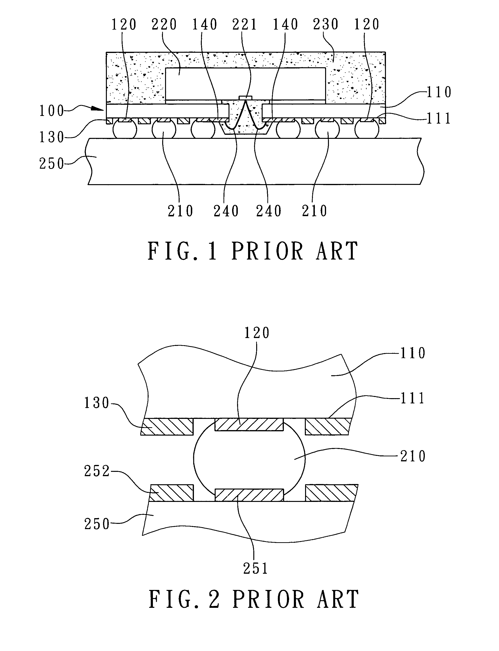
a technology of immobilization and substrate, applied in the direction of printed circuit, sustainable manufacturing/processing, final product manufacturing, etc., can solve the problems of affecting the wiring disposition of the bga package substrate, bad reliability or component failure, and serious problems, and achieve the effect of improving the immobilization of ball pads
- Summary
- Abstract
- Description
- Claims
- Application Information
AI Technical Summary
Benefits of technology
Problems solved by technology
Method used
Image

Examples
first embodiment
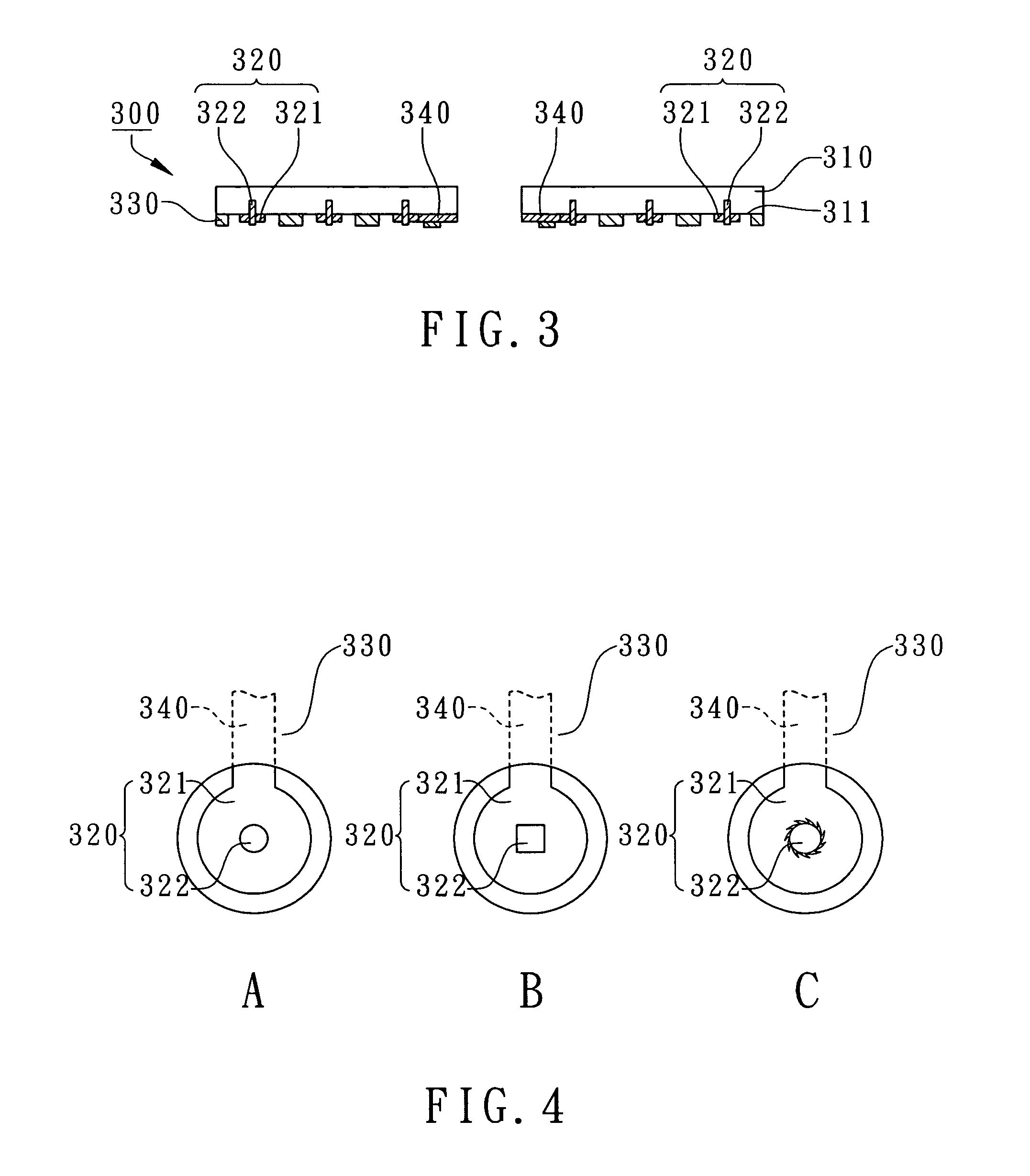
[0027]A substrate improving immobilization of ball pads for BGA packages is disclosed within the present invention to function as a chip carrier of semiconductor package. Referring to FIG. 3, the BGA package substrate 300 mainly comprises a substrate core 310, a plurality of ball pads 320 and a solder resist layer 330. In this embodiment, the BGA package substrate 300 has a single layer wiring pattern, which may adopt printed circuit board, ceramic carrier or flexible circuit film. The ball pads 320 can be arranged in an array on a same surface with the substrate core 310. In addition, “a substrate core 310” means at least a layer of substrate core, maybe two, three or more layers are included.
[0028]The substrate core 310 has a surface 311 to dispose the ball pads 320 and patterned traces (not showed in the drawings) and form a solder resist layer 330. Referring now to FIG. 6, each of the ball pads 320 has a metal pad 321 that is adhered onto the surface 311 of the substrate core 31...
second embodiment
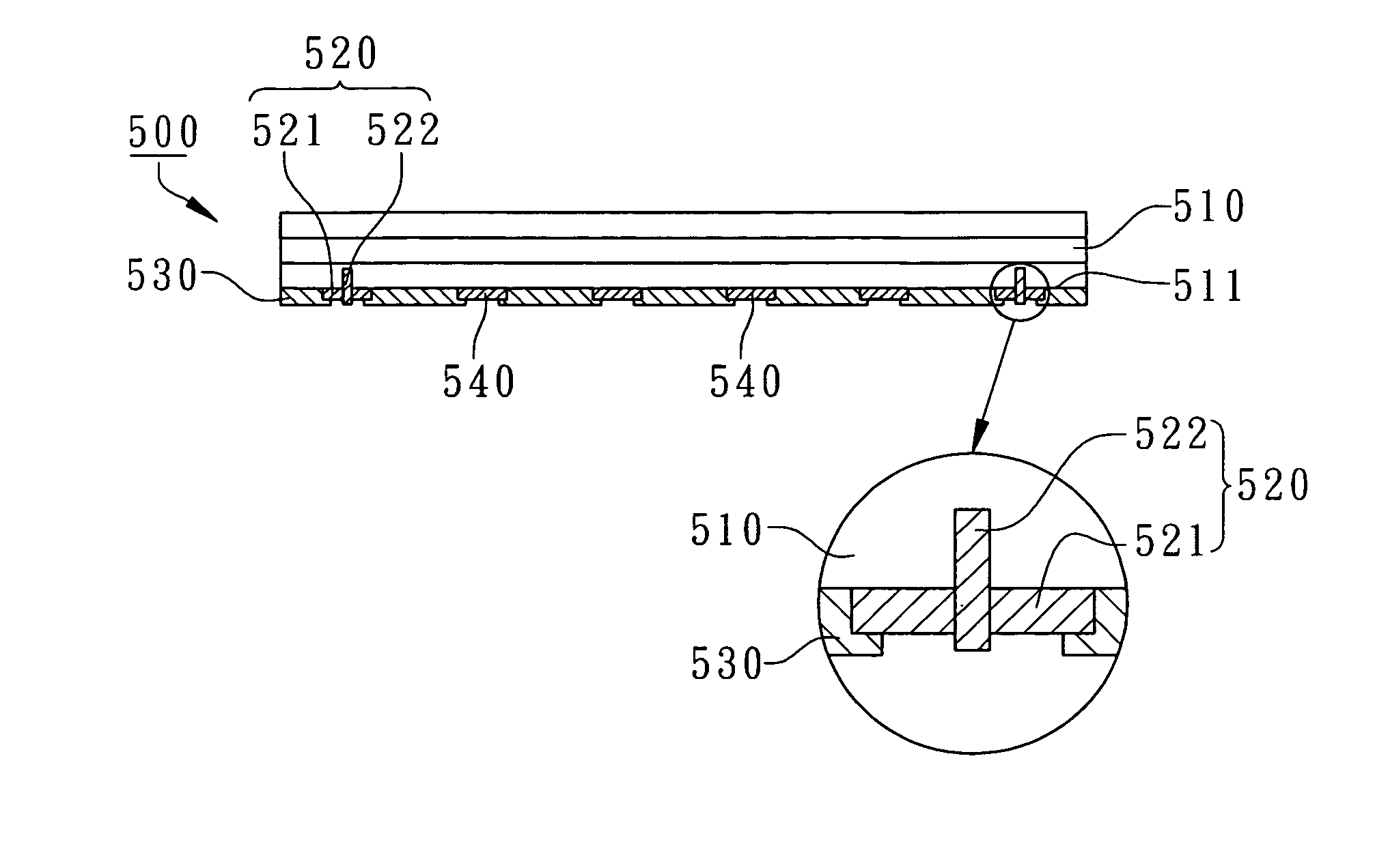
[0034]In the second embodiment, another substrate improving immobilization of ball pads for BGA packages is disclosed to illustrate that the foregoing ball pads with special shapes can be selectively disposed. Referring now to FIG. 7, the BGA package substrate 500 mainly comprises at least a substrate core 510, a plurality of ball pads 520, 540 and a solder resist layer 530. In this embodiment, partial ball pads marked with reference number “540” may generally be round pads with electrical transmission and partial ball pads marked with reference number “520” may be dummy pads without function of electrical transmission.
[0035]Within the partial ball pads 520, each of the ball pads 520 has a metal pad 521 and at least a metal nail 522. The metal pads 521 are disposed on a surface 511 of the substrate core 510 and the metal nails 522 are embedded into the substrate core 510 to improve immobilization on substrate. In this embodiment, the ball pads 540 are arranged in an array. The ball ...
PUM
| Property | Measurement | Unit |
|---|---|---|
| electrical transmission | aaaaa | aaaaa |
| shapes | aaaaa | aaaaa |
| length | aaaaa | aaaaa |
Abstract
Description
Claims
Application Information