Charge trap memory device comprising composite of nanoparticles and method of fabricating the charge trap memory device

a charge trap and memory device technology, applied in nanoinformatics, instruments, transistors, etc., can solve the problems of shortening the information retention time, increasing the leakage current to the tunneling between the nanoparticles, and poor memory performan

Active Publication Date: 2009-01-27
SAMSUNG ELECTRONICS CO LTD
View PDF46 Cites 27 Cited by
  • Summary
  • Abstract
  • Description
  • Claims
  • Application Information

AI Technical Summary

Benefits of technology

[0011]The present invention provides a charge trap memory device using a composite of charge trapping nanoparticles and insulating nanoparticles and a method of fabricating the charge trap memory device. The charge trap memory device does not have a problem of leakage current increase or nanoparticle agglomeration, which occur when an electron trap layer is formed of only metal or semiconductor nanoparticles.
[0017]The insulating nanoparticles ensure a distance between the charge trapping nanoparticles to prevent an increase in leakage current or the agglomeration of the charge trapping nanoparticles. The insulating nanoparticles can be at least one kind of nanoparticles selected from the group consisting of oxide nanoparticles including ZnO, ZrO2, SiO2, SnO2, TiO2, HfO2, BaTiO3, CeO2, Al2O3, Ta2O5, and In2O3; nitride nanoparticles including silicon nitride and silicon oxynitride; nanoparticles including C(carbon or diamond); Group II-V compound semiconductor nanoparticles; and Group III-V compound semiconductor nanoparticles. To improve memory characteristics, the insulating nanoparticles may have a larger energy band gap than the charge trapping nanoparticles. When the same kinds of nanoparticles are used as the charge trapping nanoparticles and the insulating nanoparticles, nanoparticles having a smaller work function act as the charge trapping nanoparticles.

Problems solved by technology

However, as the density of nanoparticles increases, the distance between the nanoparticles becomes shorter, thereby increasing a leakage current to the tunneling between the nanoparticles.
A larger leakage current leads to shorter information retention time and poor memory performance.
In addition, a higher density of nanoparticles leads to the agglomeration of the metal nanoparticles in a memory manufacturing process and lowers the performance of the memory device.

Method used


Image

  • Charge trap memory device comprising composite of nanoparticles and method of fabricating the charge trap memory device
  • Charge trap memory device comprising composite of nanoparticles and method of fabricating the charge trap memory device
  • Charge trap memory device comprising composite of nanoparticles and method of fabricating the charge trap memory device

Examples


Embodiment Construction

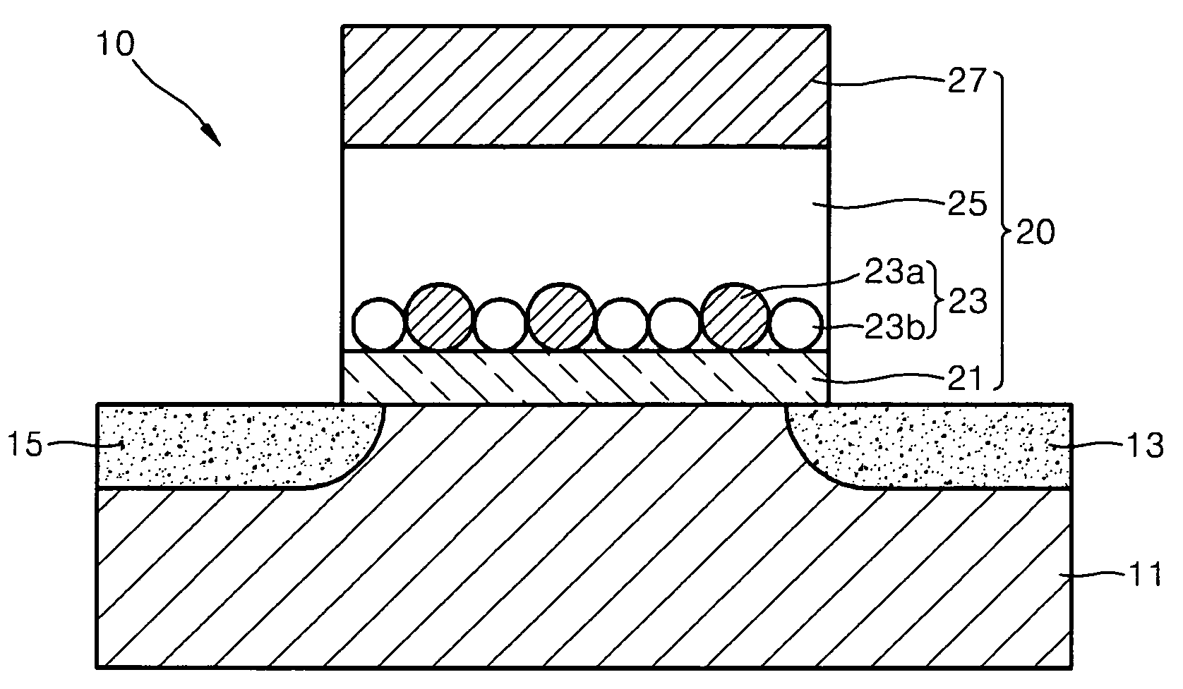
[0032]Embodiments of a charge trap memory device including a composite of nanoparticles and a method of fabricating the charge trap memory device according to the present invention will be described in detail with reference to the appended drawings.

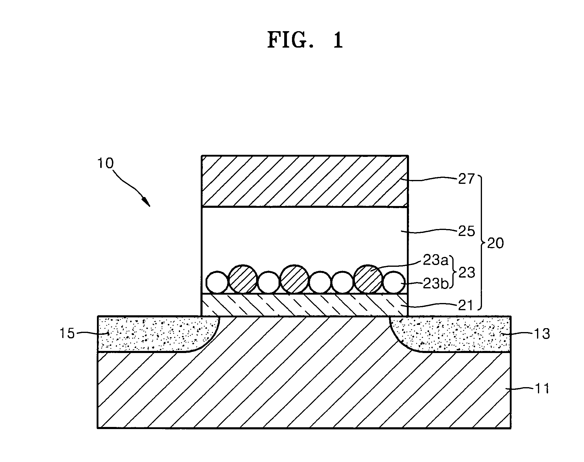
[0033]FIG. 1 is a schematic view of a charge trap memory device 10 according to an embodiment of the present invention. In FIG. 1, the thicknesses of layers and regions are exaggerated for clarity.

[0034]Referring to FIG. 1, the charge trap memory device 10 includes a substrate 11 and a gate structure 20 formed on the substrate 11.

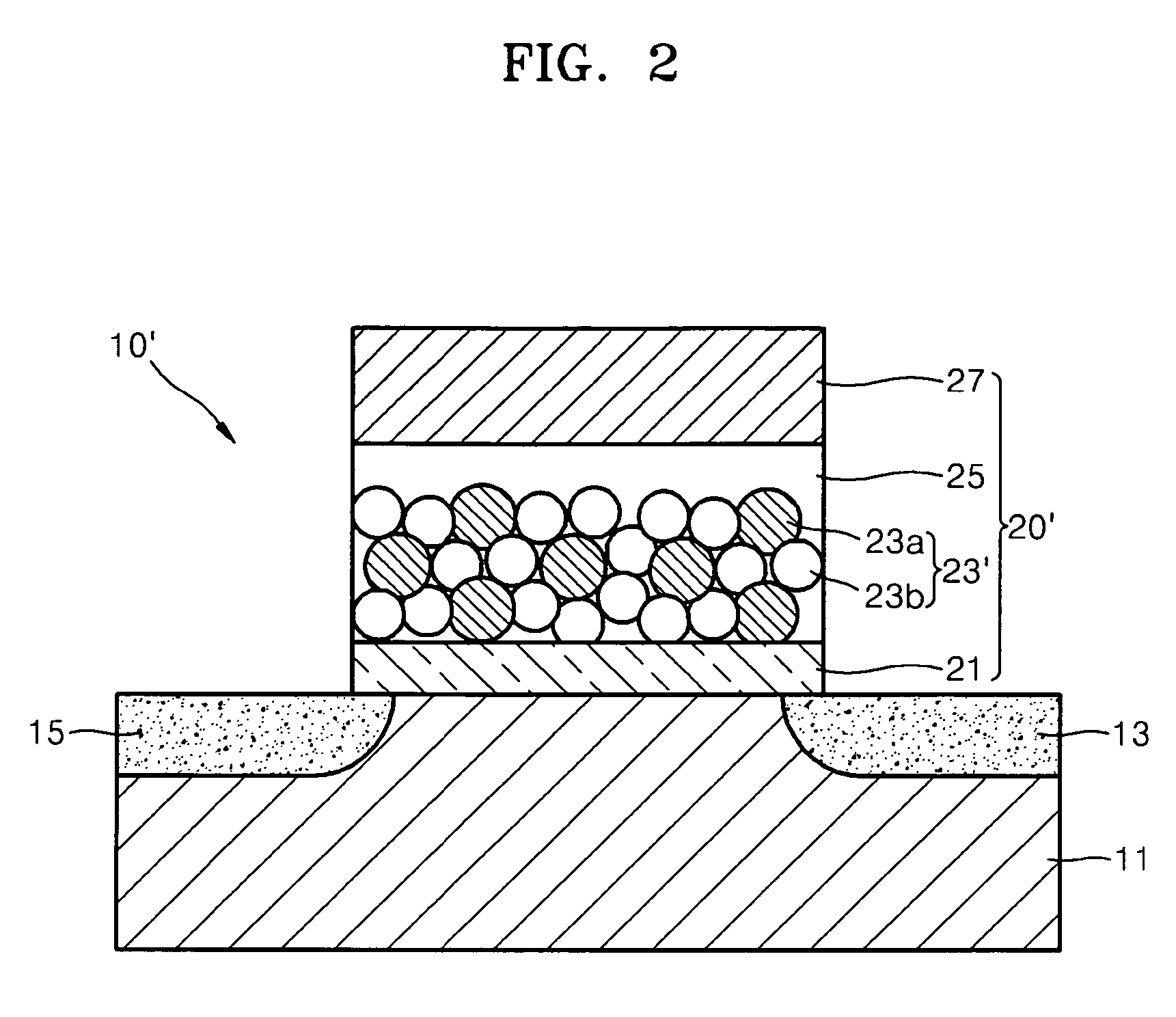
[0035]First and second impurity regions 13 and 15 doped with predetermined conductive impurities are formed in the substrate 11. One of the first and second impurity regions 13 and 15 can be used as a drain D, and the other one can be used as a source S. The gate structure 20 includes a charge trapping layer 23. A tunnel insulating layer 21 is formed between the substrate 11 and the charge trapping layer 23. The ...


PUM


Abstract

Provided are a charge trap memory device including a substrate and a gate structure including a charge trapping layer formed of a composite of nanoparticles, and a method of manufacturing the charge trap memory device.

Description

CROSS-REFERENCE TO RELATED PATENT APPLICATIONS[0001]This application claims the benefit of Korean Patent Application Nos. 10-2005-0083324 and 10-2006-0085295, filed on Sep. 7, 2005 and Sep. 5, 2006, in the Korean Intellectual Property Office, the disclosure of which is incorporated herein in its entirety by reference.BACKGROUND OF THE INVENTION[0002]1. Field of the Invention[0003]The present invention relates to a memory device and a method of fabricating the same, and more particularly, to a charge trap memory device using a composite of nanoparticles and a method of fabricating the charge trap memory device.[0004]2. Description of the Related Art[0005]Non-volatile memory devices are a data storing device that can retain stored data without loss even when the supply of power is interrupted. Flash memory device are a representative example of non-volatile memory device.[0006]Flash memory devices can be classified into either floating gate memory devices in which charges are accumula...

Claims


Application Information

Patent Timeline
Patent Type & Authority Patents(United States)
IPC IPC(8): H01L29/06H01L29/788H01L31/00
CPCB82Y10/00G11C16/0466H01L21/28273H01L29/42332H01L29/7881G11C2216/06Y10S438/962H01L29/40114
Inventor SEOL, KWANG-SOOJUN, SHIN-AEJANG, EUN-JOOLIM, JUNG-EUNCHO, KYUNG-SANGKIM, BYUNG-KILEE, JAE-HOCHOI, JAE-YOUNG
Owner SAMSUNG ELECTRONICS CO LTD
Why Eureka
Try Eureka