
Single chip GSM/EDGE transceiver architecture with closed loop power control

a transceiver and single chip technology, applied in the field of transceiver architecture, can solve the problems of consuming significantly more power, inefficient highly linear power amplifiers, and difficult to adapt existing gsm transmitter hardware to transmit signals

Inactive Publication Date: 2009-01-27
INTEL CORP
View PDF34 Cites 60 Cited by
  • Summary
  • Abstract
  • Description
  • Claims
  • Application Information

AI Technical Summary

Problems solved by technology

Unfortunately, existing GSM transmitter hardware is not easily adapted to transmit a signal that includes both a PM component and an AM component.
Unfortunately, highly linear power amplifiers are very inefficient, thus consuming significantly more power than a non-linear power amplifier and drastically reducing the life of the battery or other power source.
This condition is further complicated because transmitters typically employed in GSM communication systems transmit in bursts and must be able to control the ramp-up of the transmit power as well as have a high degree of control over the output power level over a wide power range.
Further, in those transmission standards in which both a PM signal and an AM signal are sent to a power amplifier, unless the power amplifier is very linear, it may distort the combined transmission signal by causing undesirable AM to PM conversion.
This conversion is detrimental to the transmit signal and can require the use of a costly and inefficient linear power amplifier.
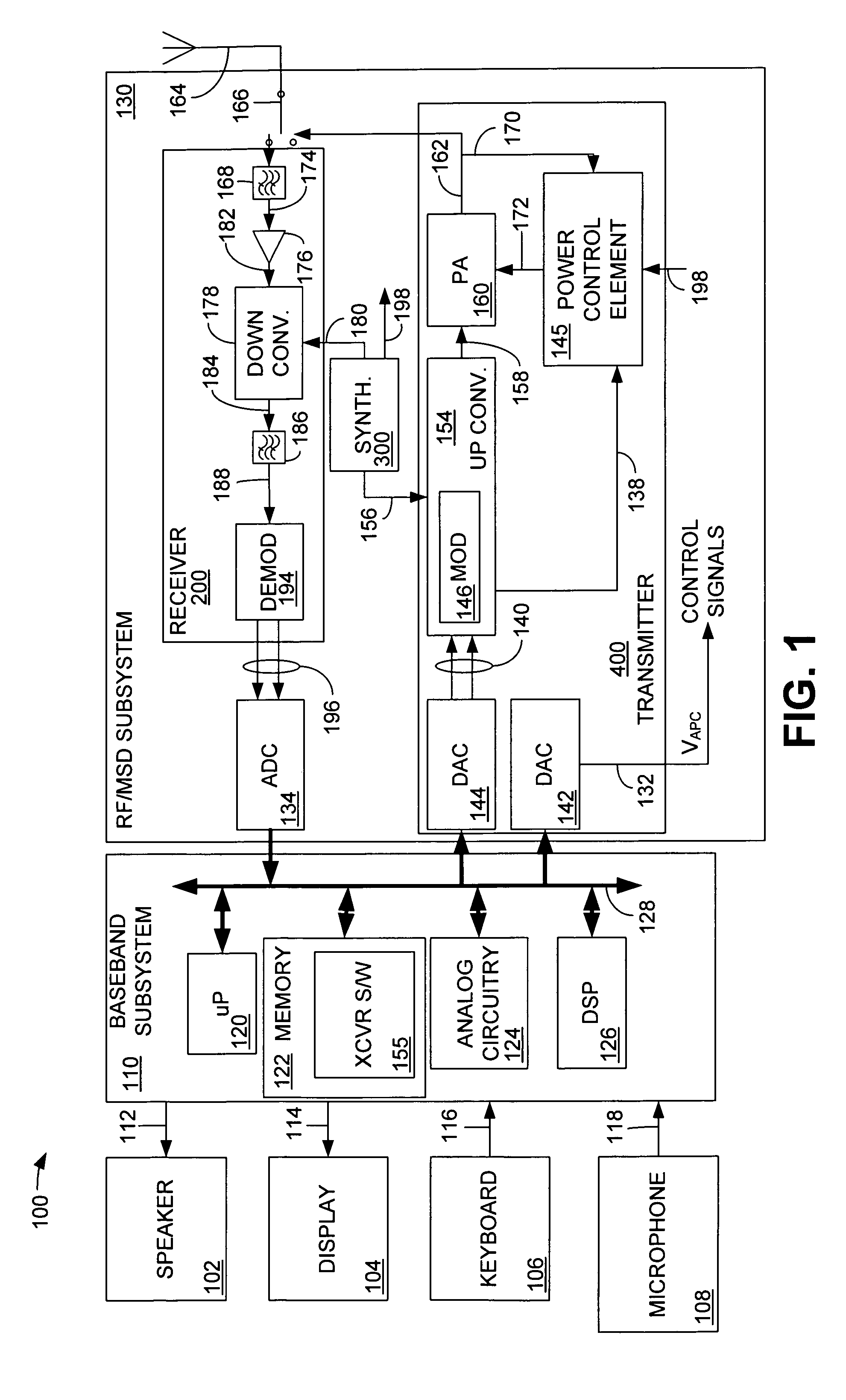
In the past, the transceiver components for such a communication system were typically implemented using multiple devices, also referred to as “chips.” However, industry pressures to reduce cost, implementation complexity and power consumption and to extend battery life are driving the industry to attempt single chip architectures.
Unfortunately, a single chip implementation for a GSM / EDGE transceiver presents many design challenges, especially in a system in which a closed power control loop is used to control output power of the transmitter.
For example, when a closed loop power control system is implemented on the same chip as the transceiver components, the radio frequency (RF) on-chip isolation requirement between the components becomes a major factor affecting transceiver performance.

Method used


Image

  • Single chip GSM/EDGE transceiver architecture with closed loop power control
  • Single chip GSM/EDGE transceiver architecture with closed loop power control
  • Single chip GSM/EDGE transceiver architecture with closed loop power control

Examples


Embodiment Construction

[0017]Although described with particular reference to a portable transceiver, the single chip GSM / EDGE transceiver architecture with closed loop power control (hereafter referred to as the “single chip GSM / EDGE transceiver”) can be implemented in any system where it is desirable to have a single chip GSM / EDGE transceiver.

[0018]The single chip GSM / EDGE transceiver can be implemented in hardware, software, or a combination of hardware and software. When implemented in hardware, the single chip GSM / EDGE transceiver can be implemented using specialized hardware elements and logic. When the single chip GSM / EDGE transceiver is implemented partially in software, the software portion can be used to precisely control the various components in the transceiver. The software can be stored in a memory and executed by a suitable instruction execution system (microprocessor). The hardware implementation of the single chip GSM / EDGE transceiver can include any or a combination of the following techn...


PUM


Abstract

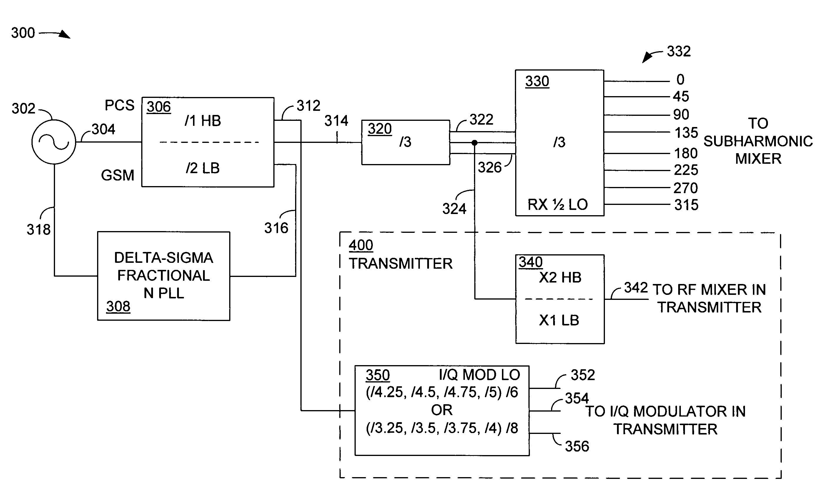
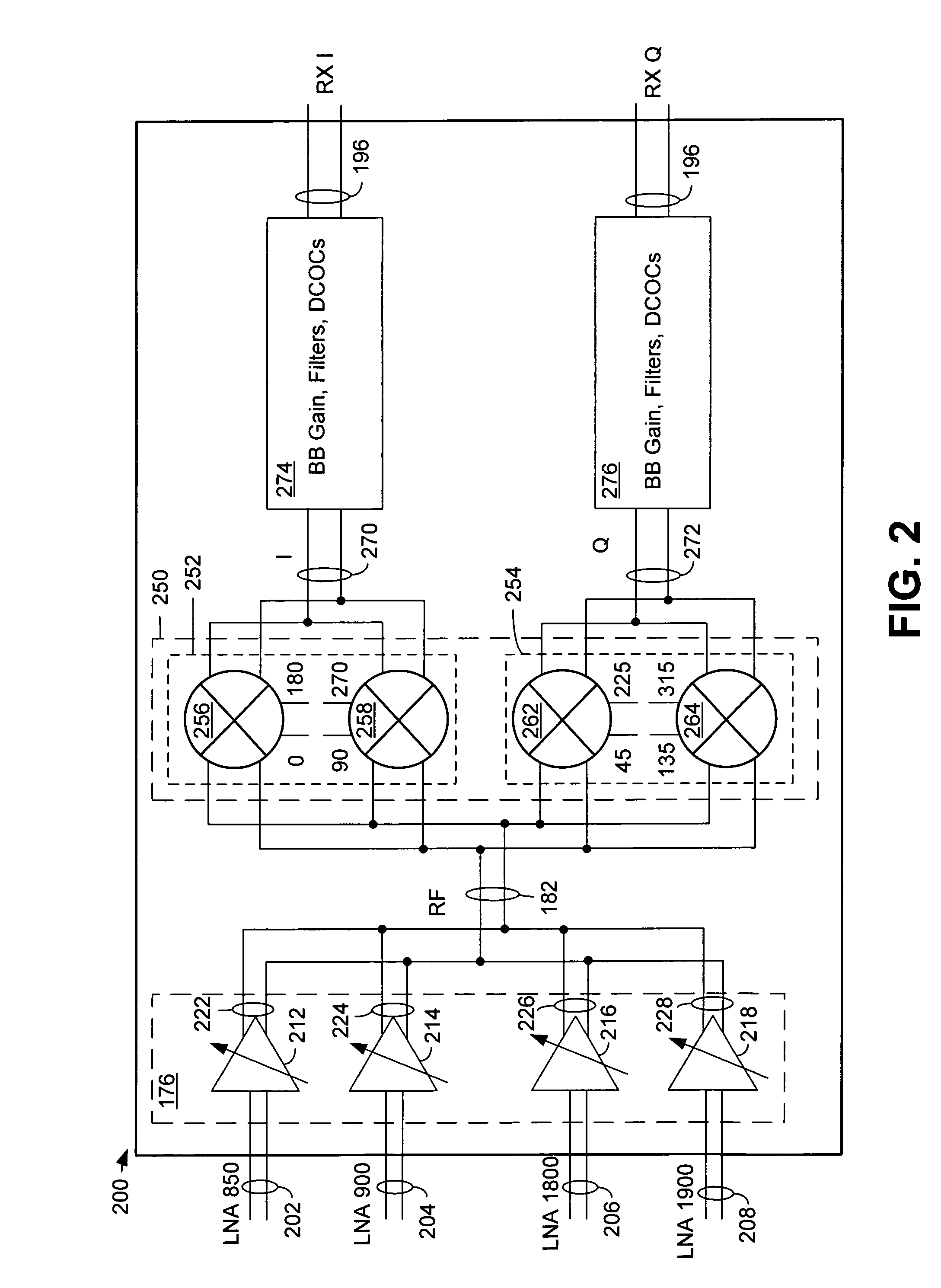
A single chip GSM / EDGE transceiver comprises a fully differential receive chain, a subharmonic mixer in the receive chain, the subharmonic mixer configured to receive a radio frequency (RF) input signal and a local oscillator (LO) signal that is phase-shifted by a nominal 45 degrees, and a synthesizer having a voltage controlled oscillator and having at least one frequency divider to generate desired transmit and receive LO signals. The transceiver also comprises a transmitter having a closed power control loop, and a harmonic rejection modulator, the use thereof made possible by a frequency plan designed to allow the synthesizer to develop the transmit and receive LO signals without a frequency multiplier.

Description

BACKGROUND[0001]1. Field of the Invention[0002]This invention relates generally to transceiver architecture in a wireless portable communication device. More particularly, the invention relates to a single chip implementation of a global system for mobile communication (GSM) / enhanced data rates for GSM evolution (EDGE), referred to as “GSM / EDGE,” transceiver having closed loop power control.[0003]2. Related Art[0004]Radio frequency (RF) transmitters are found in many one-way and two-way communication devices, such as portable communication devices, (cellular telephones), personal digital assistants (PDAs) and other communication devices. An RF transmitter must transmit using whatever communication methodology is dictated by the particular communication system within which it is operating. For example, communication methodologies typically include amplitude modulation, frequency modulation, phase modulation, or a combination of these. In a typical global system for mobile communicati...

Claims


Application Information

Patent Timeline
Patent Type & Authority Patents(United States)
IPC IPC(8): H04B1/38
CPCH03B19/14H03G3/3047H03L7/081H03L7/23H03L7/0992H03L7/1978H03L7/087H03D7/00
Inventor ROZENBLIT, DMITRIYSOWLATI, TIRDADPULLELA, RAJASEKHAR
Owner INTEL CORP
Learn More