
Array substrate for liquid crystal display device and the seal pattern in the periphery of the display

a liquid crystal display and substrate technology, applied in the field of display devices, can solve the problems of affecting the adhesion of the seal pattern of the dummy pattern to the possibility of corrosion along the gate link line b>14/b>, and the migration of a metallic material between the metal pattern of the dummy pattern and the gate link line, so as to improve the adhesion of the seal pattern, reduce manufacturing costs, and simplify manufacturing processes

Inactive Publication Date: 2009-02-03
LG DISPLAY CO LTD
View PDF3 Cites 2 Cited by
  • Summary
  • Abstract
  • Description
  • Claims
  • Application Information

AI Technical Summary

Benefits of technology

[0020]An object of the present invention is to provide an array substrate for a liquid crystal display device and a manufacturing method of the same that improve adhesion of a seal pattern.
[0021]Another object of the present invention is to provide an array substrate for a liquid crystal display device and a manufacturing method of the same that reduce manufacturing costs, simplify manufacturing processes and prevent electrical short.

Problems solved by technology

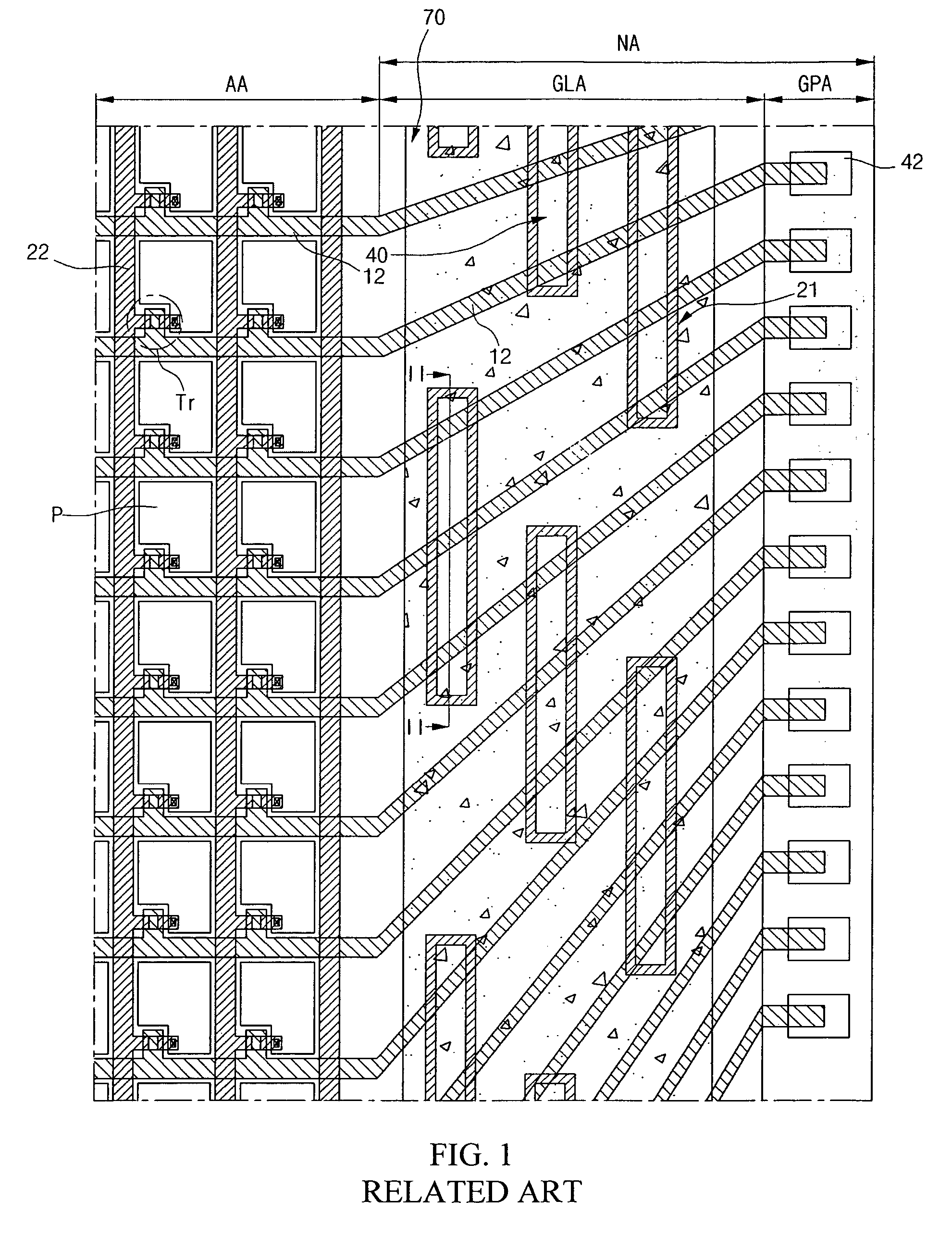
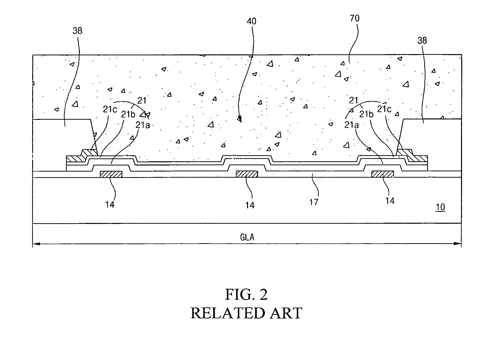
As a result, corrosion along the gate link line 14 is likely to occur.
Nonetheless, there may be electrical short between the metal pattern of the dummy pattern and the gate link lines.
The pressure can create cracks in the gate insulating layer and result hillock or migration of a metallic material for the gate link lines being in the cracks.
Such metallic materials can contact the metal pattern of the dummy pattern causing an electric short and creating a defect.

Method used


Image

  • Array substrate for liquid crystal display device and the seal pattern in the periphery of the display
  • Array substrate for liquid crystal display device and the seal pattern in the periphery of the display
  • Array substrate for liquid crystal display device and the seal pattern in the periphery of the display

Examples


Embodiment Construction

[0035]Reference will now be made in detail to preferred embodiments of the present invention, examples of which are illustrated in the accompanying drawings.

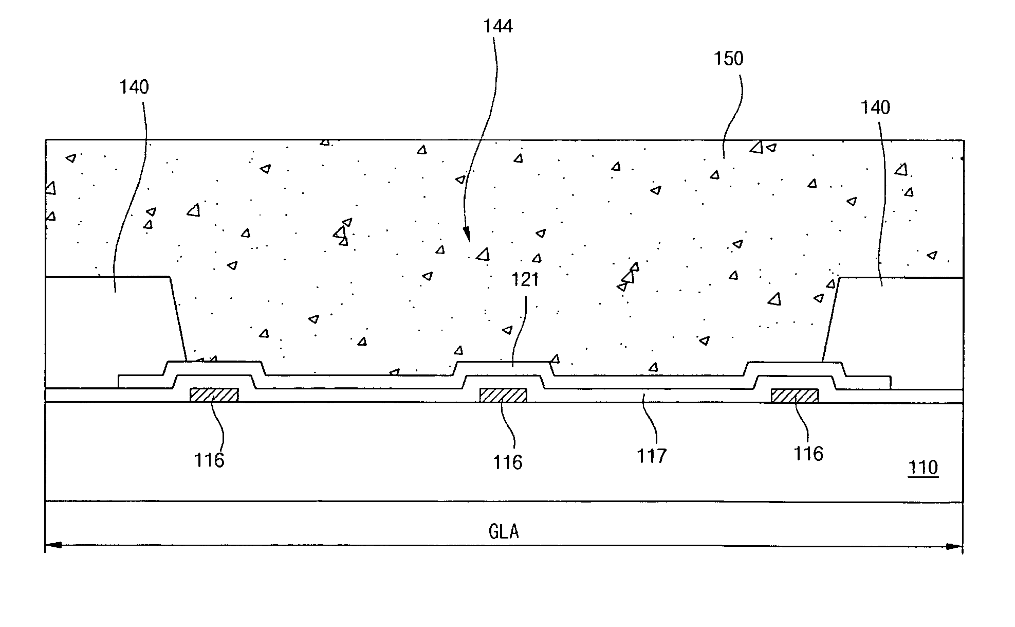
[0036]FIG. 3 is a plan view illustrating an array substrate for an LCD device according to an embodiment the present invention. In FIG. 3, the array substrate includes a display area AA and a non-display area NA. The non-display area NA includes a gate link region GLA, a gate pad region GPA, a data link region (not shown), and a data pad region (not shown).

[0037]In the display area AA, gate lines 112 are formed in a horizontal direction in the context of the figure, and data lines 125 are formed in a vertical direction in the context of the figure. The gate lines 112 and the data lines 125 cross each other to define pixel regions P, and a thin film transistor Tr is formed at each crossing of the gate lines 112 and the data lines 125. A pixel electrode 145 is formed at each pixel region P and is connected to the thin film transis...


PUM


Abstract

A substrate for a display device includes a plurality of first lines on the substrate in a display area of the display device, a plurality of link lines on the substrate in a link region, the link lines electrically connected to the first lines and the link region being in a non-display area of the display device, an insulating layer on the first lines and the link lines, a plurality of second lines on the insulating layer, patterns on the insulating layer in the link region and at least partially overlapping the link lines, the patterns including an intrinsic semiconductor material, and a passivation layer on the second lines and the patterns, the passivation layer having at least one through hole exposing the intrinsic semiconductor material of at least one of the patterns.

Description

[0001]The present invention claims the benefit of Korean Patent Application No. 2005-0097475 filed in Korea on Oct. 17, 2005, which is hereby incorporated by reference.BACKGROUND OF THE INVENTION[0002]1. Field of the Invention[0003]The present invention relates to a display device, and more particularly, relates to an array substrate for a liquid crystal display (LCD) device and a manufacturing method of the same.[0004]2. Discussion of the Related Art[0005]Our information-based society has an increasing demand for flat panel display (FPD) devices. FPD devices include plasma display panel (PDP) devices, field emission display (FED) devices, electroluminescent display (ELD) devices, liquid crystal display (LCD) devices, and so on. Since they are small and lightweight and have low power consumption, FPD devices are taking the place of cathode ray tube (CRT) display devices.[0006]Among the various FPD devices, LCD devices are particularly useful in notebook computers and desktop monitor...

Claims


Application Information

Patent Timeline
Patent Type & Authority Patents(United States)
IPC IPC(8): H01L31/062H01L31/113
CPCG02F1/1345G02F1/133345G02F1/1339H01L27/1288G02F1/136
Inventor LEE, JU-BOKLEE, JAE-GU
Owner LG DISPLAY CO LTD
Learn More