Linear low capacitance overvoltage protection circuit

a protection circuit and low capacitance technology, applied in the direction of overvoltage protection resistors, emergency protection arrangements for limiting excess voltage/current, etc., can solve the problems of suboptimal channel performance, intermodulation distortion, and capacitors whose values vary with voltage, and achieve the effect of minimizing the capacitance of the diodes

Active Publication Date: 2009-04-07
LITTELFUSE INC
View PDF28 Cites 8 Cited by
  • Summary
  • Abstract
  • Description
  • Claims
  • Application Information

AI Technical Summary

Benefits of technology

[0011]In accordance with another feature of the invention, disclosed is an overvoltage protection circuit having at least two terminals. The overvoltage protection device is responsive to an overvoltage for providing a low impedance path between the two terminals. The overvoltage protection device is characterized by a surge current. Provided is a diode bridge with at least four diodes and having a first node and a second node. The overvoltage protection device is connected between the first and second nodes of the diode bridge. Some of the diodes have junction areas for carrying the surge currents of the overvoltage protection device and not substantially larger, thereby minimizing a capacitance of the diodes.

Problems solved by technology

Capacitors whose values vary with voltage are inherently nonlinear devices.
In other words, a bipolar overvoltage protection device placed across a circuit to be protected can affect the operation of the circuit even if the overvoltage protection device remains in its off state.
The non-linearity can lead to suboptimal channel performance and intermodulation distortion.
The adverse affects of the foregoing are experienced in many applications, including communication lines where overvoltage protection circuits are routinely employed to protect transmitting and receiving circuits from high voltages that may be inadvertently coupled to the communication lines.
The adverse affects of the use of silicon bipolar overvoltage protection devices may not arise from the fact that such devices have an inherent capacitance, but rather from the characteristic that such capacitance changes as a function of the voltage applied across the device.
It can be seen that if the electrical state of the line changes after the equalization session, the transmission data rate may not be optimized, and thus transmission errors can occur.
As a result, the data receiver or modem at the receiving end of the communication line may detect errors arising from the transmission of data at a rate higher than the line can reliably carry in the off-hook condition.
The excessive error rate may cause the modem to retrain, which results in a temporary loss of service during retraining, which is unacceptable.

Method used


Image

  • Linear low capacitance overvoltage protection circuit
  • Linear low capacitance overvoltage protection circuit
  • Linear low capacitance overvoltage protection circuit

Examples


Embodiment Construction

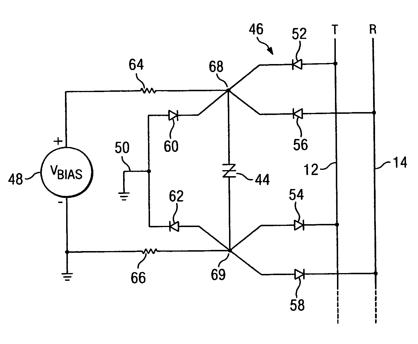
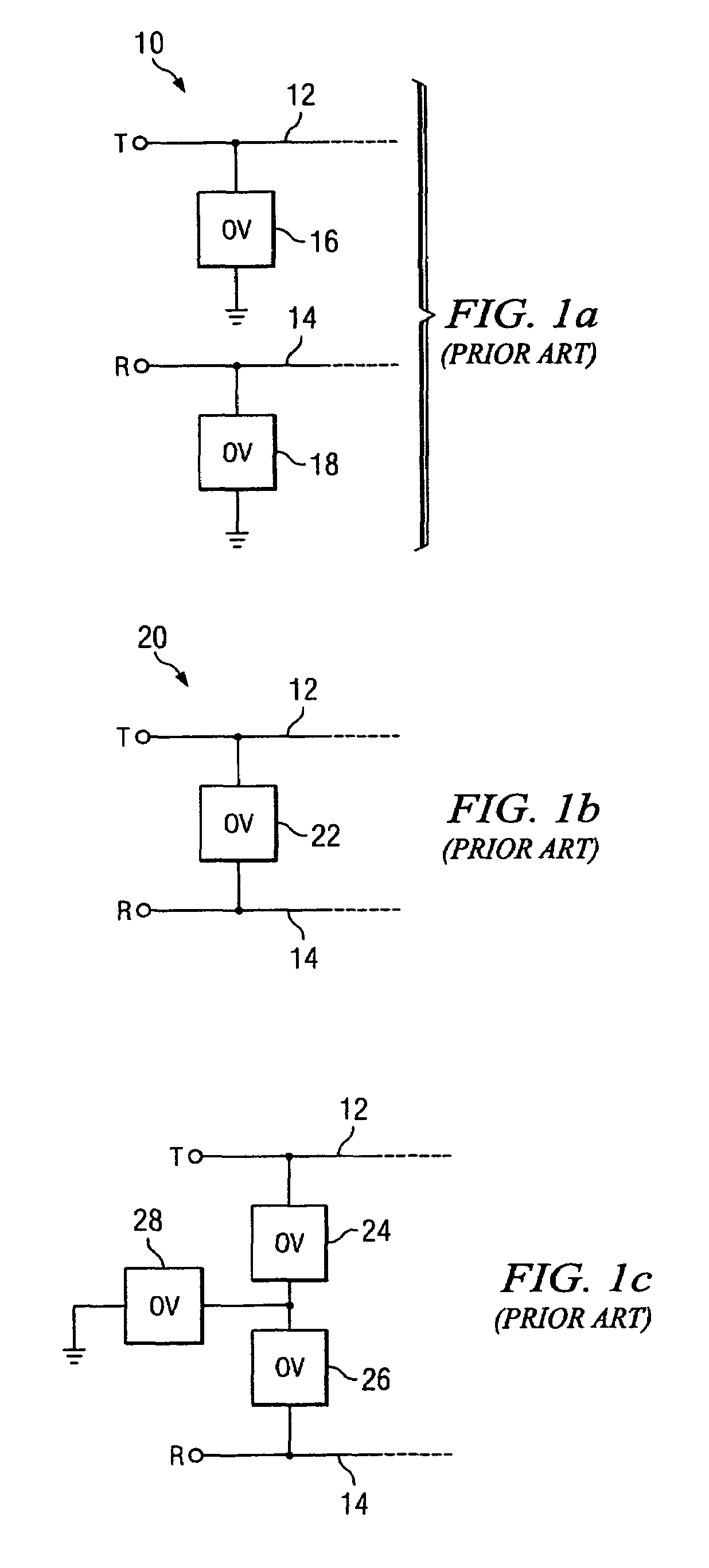
[0026]Referring to FIG. 1a of the drawings, there is shown an environment 10 in which the invention can be advantageously practiced. Here, the communication line includes a tip conductor 12 and a ring conductor 14. An overvoltage protection device 16 is connected between ground, or some other voltage source, and the tip conductor 12 to provide overvoltage protection to such conductor 12. The ring conductor 14 is similarly connected to overvoltage protection device 18 to provide overvoltage protection thereto. In this circuit 10, both overvoltage protection devices 16 and 18 are preferably bidirectional devices constructed on the same silicon chip so as to present balanced electrical characteristics to both communication line conductors 12 and 14. The bidirectional characteristics of the overvoltage protection devices 16 and 18 provide overvoltage protection for both polarities of overvoltages. In addition, it is preferable that both overvoltage protection devices 16 and 18 have brea...


PUM


Abstract

A bipolar semiconductor overvoltage protection circuit presents less capacitance to a communication line. The overvoltage protection circuit includes an overvoltage protection device that is biased with a voltage to not only reduce the capacitance thereof, but also to reduce the change in capacitance as a function of frequency. Changes in communication line voltages thus change the capacitance of the overvoltage protection device less, resulting in the ability to allow the transmission of high capacity data protocols with reduced error rates.

Description

TECHNICAL FIELD OF THE INVENTION[0001]The present invention relates in general to overvoltage protection devices and circuits, and more particularly to overvoltage protection circuits providing reduced capacitance changes in circuits that experience changing voltages.RELATED APPLICATIONS[0002]This non-provisional patent application is related to U.S. patent application entitled “Stacked Integrated Circuit Chip Assembly” by Chad A. Vos, Ser. No. 11 / 254,163, filed on even date herewith. This non-provisional patent application is also related to U.S. patent application entitled “Integrated Circuit Providing Overvoltage Protection For Low Voltage Lines” by Chad A. Vos and Kelly C. Casey, Ser. No. 11 / 254,163, filed on even date herewith.BACKGROUND OF THE INVENTION[0003]Many circuits in electronic equipment provide protection from the harmful effects of overvoltages, overcurrents, etc. These protection circuits are often designed as an integral part of the general electronic circuit, but ...

Claims


Application Information

Patent Timeline
Patent Type & Authority Patents(United States)
IPC IPC(8): H02H9/04H02H1/04H04M1/00H02H3/22
CPCH04M3/18
Inventor CASEY, KELLY C.
Owner LITTELFUSE INC
Why Eureka
Try Eureka