
Memory architecture of 3D array with improved uniformity of bit line capacitances
a memory architecture and capacitance technology, applied in the field of memory devices with high density, can solve the problems of limiting the number of control gates that can be layered in this way, the structure is not symmetrical for different locations of the array, and the manufacturing cost limit the use of technology, etc., to achieve stable sensing margins and minimize the capacitance different of each metal bit line.
- Summary
- Abstract
- Description
- Claims
- Application Information
AI Technical Summary
Benefits of technology
Problems solved by technology
Method used
Image

Examples
Embodiment Construction
[0092]A detailed description of embodiments is provided with reference to the Figures.
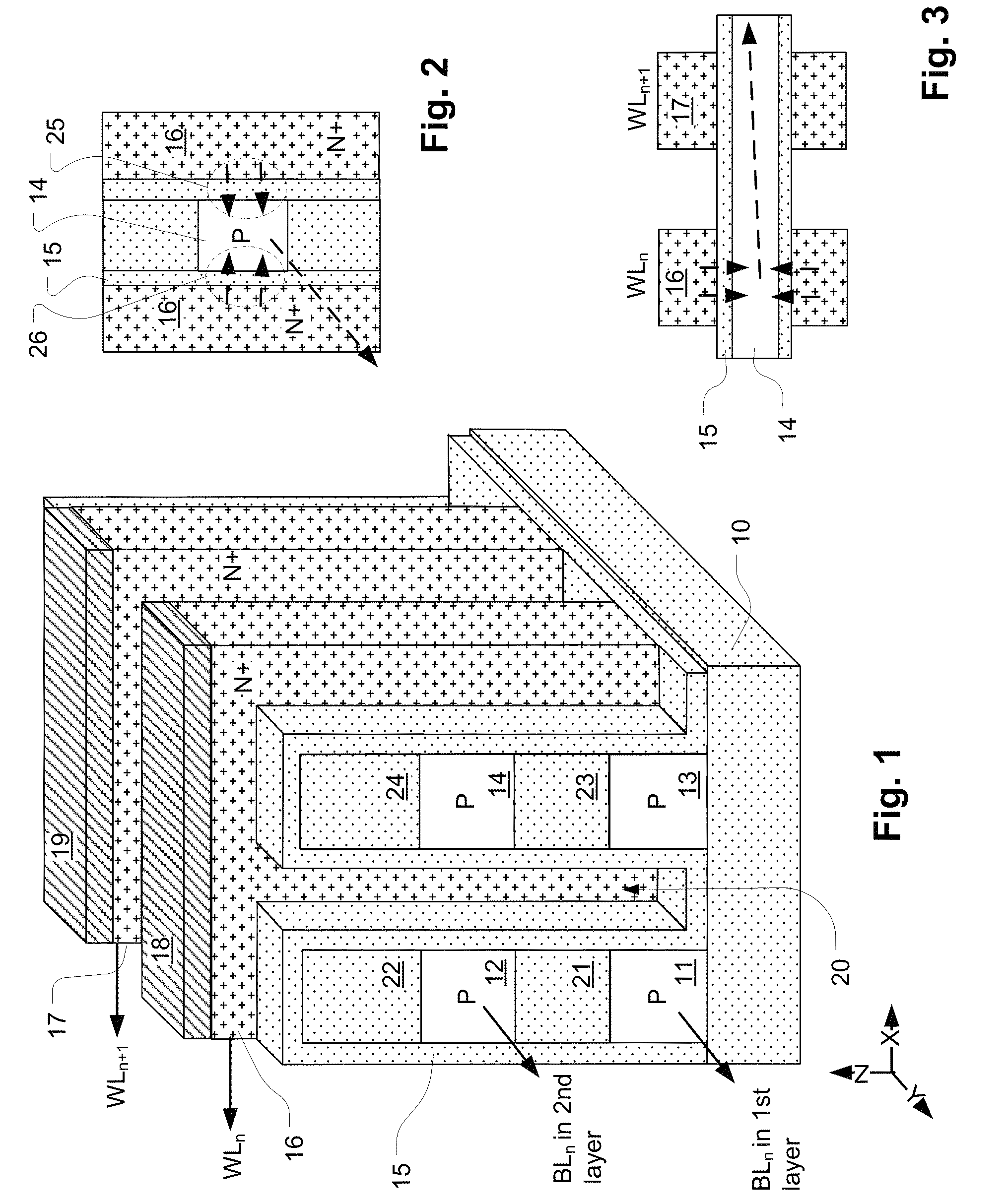
[0093]FIG. 1 is a perspective drawing of a 2×2 portion of a three-dimensional programmable resistance memory array with fill material removed from the drawing to give a view of the stacks of semiconductor strips and orthogonal word lines that make up the 3D array. In this illustration, only 2 planes are shown. However, the number of planes can be extended to very large numbers. As shown in FIG. 1, the memory array is formed on an integrated circuit substrate having an insulating layer 10 over underlying semiconductor or other structures (not shown). The memory array includes a plurality of stacks of semiconductor strips 11, 12, 13, 14 separated by insulating material 21, 22, 23, 24. The stacks are ridge-shaped extending on the Y-axis as illustrated in the figure, so that the semiconductor strips 11-14 can be configured as memory cell strings. Semiconductor strips 11 and 13 can act as memory cell st...
PUM
 Abstract
Description
Claims
Application Information