Film bulk acoustic resonator (FBAR) and preparation method thereof

A thin-film bulk acoustic wave and resonator technology, applied in the field of microelectronics, can solve the problems of large silicon integrated circuits, insufficient reliability, and low yield, and achieve improved circuit performance, convenient sensing, and strong mechanical fastness. Effect

Inactive Publication Date: 2010-01-20
ZHEJIANG UNIV +1
View PDF2 Cites 28 Cited by
  • Summary
  • Abstract
  • Description
  • Claims
  • Application Information

AI Technical Summary

Problems solved by technology

In 2008, the patent document WO 2008 / 101646A1 proposed a monolithic integration technology, which is to invert the FBAR, use a metal layer to support the electrical contact of the CMOS circuit, and form an air gap structure. This method can further reduce the chip area, but still requires Two sets of different processes prepare FBAR and CMOS circuits separately, and this method uses a support structure, the reliability is not high enough, and the yield will be relatively low
The above integration technologies all require a single silicon chip area for manufacturing FBAR, which is fabricated on a single silicon chip, and the general area of ​​FBAR is 1 to 5×10 4 um 2 , which is too large and expensive for a silicon integrated circuit

Method used


Image

  • Film bulk acoustic resonator (FBAR) and preparation method thereof
  • Film bulk acoustic resonator (FBAR) and preparation method thereof

Examples


Embodiment Construction

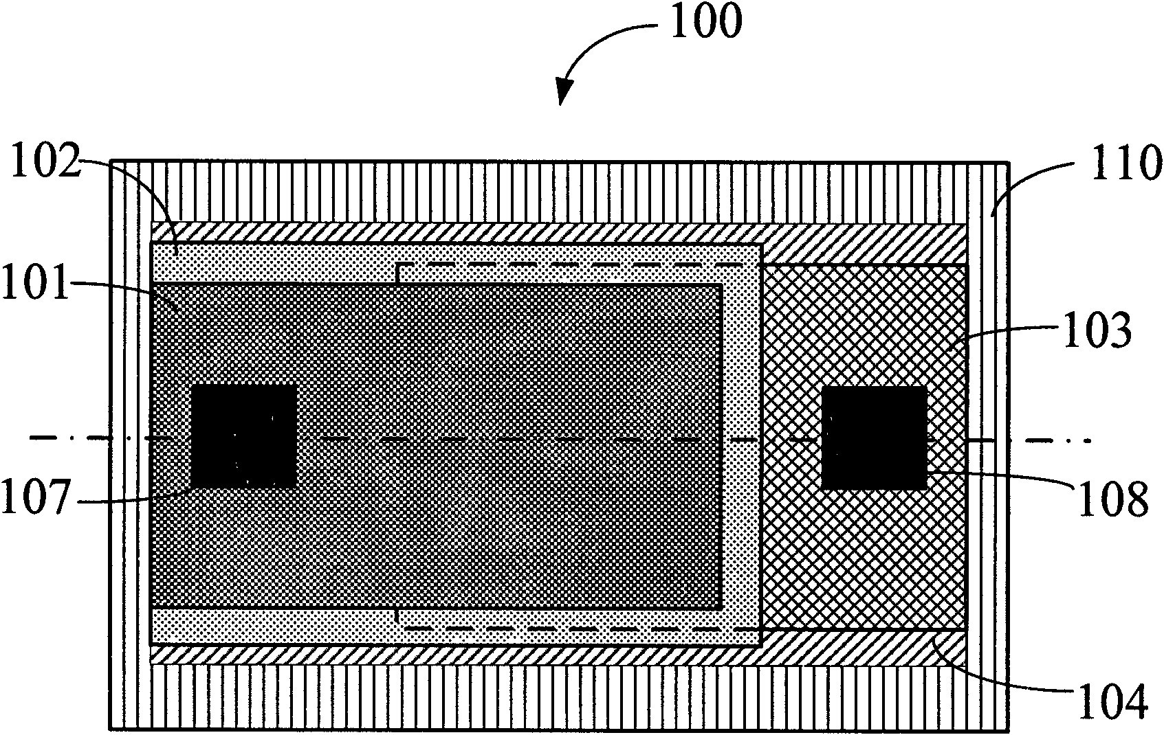
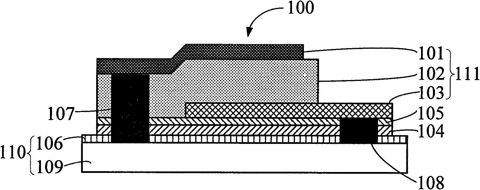
[0022] see figure 1 , a schematic top view of the integrated structure of the FBAR with a Bragg reflective layer of the present invention, figure 2 is a schematic cross-sectional view of an integrated structure of an FBAR using a Bragg reflection layer according to an embodiment of the present invention.

[0023] The FBAR in the figure includes a substrate 110 , an acoustic wave reflection layer on it and a sandwich piezoelectric stack 111 , and the acoustic wave reflection layer in the figure is composed of a layer of low acoustic impedance film 104 and a layer of high acoustic impedance film 105 .

[0024] The substrate 110 is composed of an integrated circuit chip 109 capable of FBAR signal processing and a passivation layer 106 deposited on the integrated circuit chip 109 and whose surface is polished.

[0025] The sandwich piezoelectric stack includes an upper electrode 101 , a lower electrode 103 and a piezoelectric layer 102 .

[0026] The sandwich piezoelectric stac...


PUM


Abstract

The invention discloses a film bulk acoustic resonator (FBAR) and a preparation method thereof. The film bulk acoustic resonator comprises a substrate, an acoustic wave reflecting layer and a sandwich piezoelectric stack which are integrated into a whole, wherein the substrate comprises an integrated circuit chip capable of carrying out FBAR signal processing and a passivation layer which is deposited on the integrated circuit chip and polished on the surface; and the acoustic wave reflecting layer and the sandwich piezoelectric stack are positioned on the surface of the passivation layer of the substrate. The FBAR does not additionally occupy the area of a silicon wafer, can greatly reduce the area and the cost of the chip, has simple and reliable structure, is convenient for sensing, is connected with a processing circuit by a communication hole, can reduce the reflection of a radio frequency signal and can be used for single-chip integrated design of a plurality of radio frequency systems and micro-quality sensing systems.

Description

technical field [0001] The invention relates to the technical field of microelectronics, in particular to a film bulk acoustic resonator FBAR and a manufacturing method thereof. Background technique [0002] Wireless communication is developing towards high communication frequency, high transmission rate, high-intensity multiplexing and high integration. At present, semiconductor technology can fully integrate active devices into a chip, but passive frequency devices cannot be integrated, which seriously restricts the development of RFIC. Passive components are mainly multiplexers, filters, resonators and matching LC networks. Resonators can form multiplexers, filters, oscillators, etc. A wireless transceiver requires multiple resonators to form multiplexers, VCO and RF filter. Therefore, the integration of the basic unit resonator is the key to the problem. At present, wireless communication requires higher-capacity data transmission in a narrow frequency band. For examp...

Claims


Application Information

Patent Timeline
Patent Type & Authority Applications(China)
IPC IPC(8): H03H9/17H03H3/02
Inventor 董树荣任天令杨轶赵士恒彭平刚
Owner ZHEJIANG UNIV
Why Eureka
Try Eureka