Method and system for reducing inter-layer capacitance in integrated circuits

a technology of inter-layer capacitance and integrated circuit, which is applied in the direction of individual semiconductor device testing, semiconductor/solid-state device testing/measurement, instruments, etc., can solve the problems of large overlap over dummy fill areas on successive layers, adverse effects of dummy filling on electric field, and inability to address unwanted bulk capacitance and the like, so as to reduce the unwanted bulk capacitance introduced by the dummy fill and minimize the effect of inter-layer capa

Active Publication Date: 2008-07-08
BELL SEMICON LLC
View PDF9 Cites 4 Cited by
  • Summary
  • Abstract
  • Description
  • Claims
  • Application Information

AI Technical Summary

Benefits of technology

[0010]Additionally, the first dummy fill pattern may be placed to form a checkerboard pattern. If the first layer is already arranged in the form of a checkerboard pattern, the first dummy fill pattern may not be re-arranged. Then, the second dummy fill pattern may be placed to form a checkerboard pattern so as to be offset from the first dummy fill pattern. In this manner, each of the dummy fill features on the first layer may not be placed directly above dummy fill features on the second layer. Consequently, the unwanted bulk capacitance introduce by the dummy fill may be reduced and thus the inter-layer capacitance is minimized.

Problems solved by technology

The bulk capacitance generated due to the overlap of signal carrying lines on Metal 1 and Metal 2 may not be easily avoided since the placement of signal carrying lines is dictated by circuit functionality.
While most dummy fills methodologies have focused on uniform feature density, the problems created by the inserted dummy fills such as adverse effects on the electric field, unwanted bulk capacitance, and the like have not been addressed.
Further, the existing dummy fill methodologies treat each layer independently which results in a large overlap over dummy fill areas on successive layers.
If the overlaps 206 are large, the unwanted bulk capacitance may be increased, thereby slowing down signals in the circuit and adversely affecting timing.

Method used


Image

  • Method and system for reducing inter-layer capacitance in integrated circuits
  • Method and system for reducing inter-layer capacitance in integrated circuits
  • Method and system for reducing inter-layer capacitance in integrated circuits

Examples


Embodiment Construction

[0019]Reference will now be made in detail to the presently preferred embodiments of the invention, examples of which are illustrated in the accompanying drawings.

[0020]Referring generally now to FIGS. 3 through 5, exemplary embodiments of the present invention are shown.

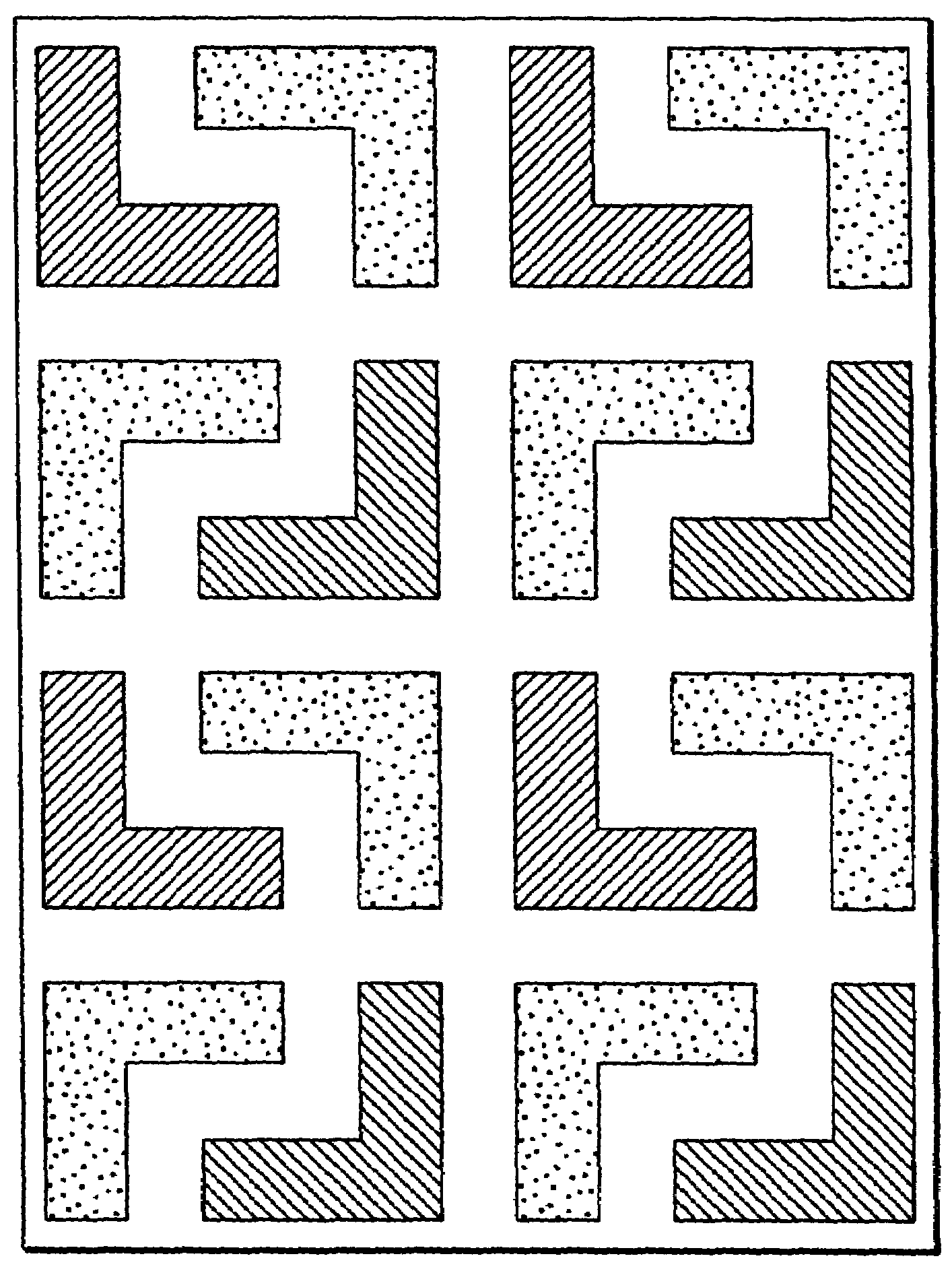
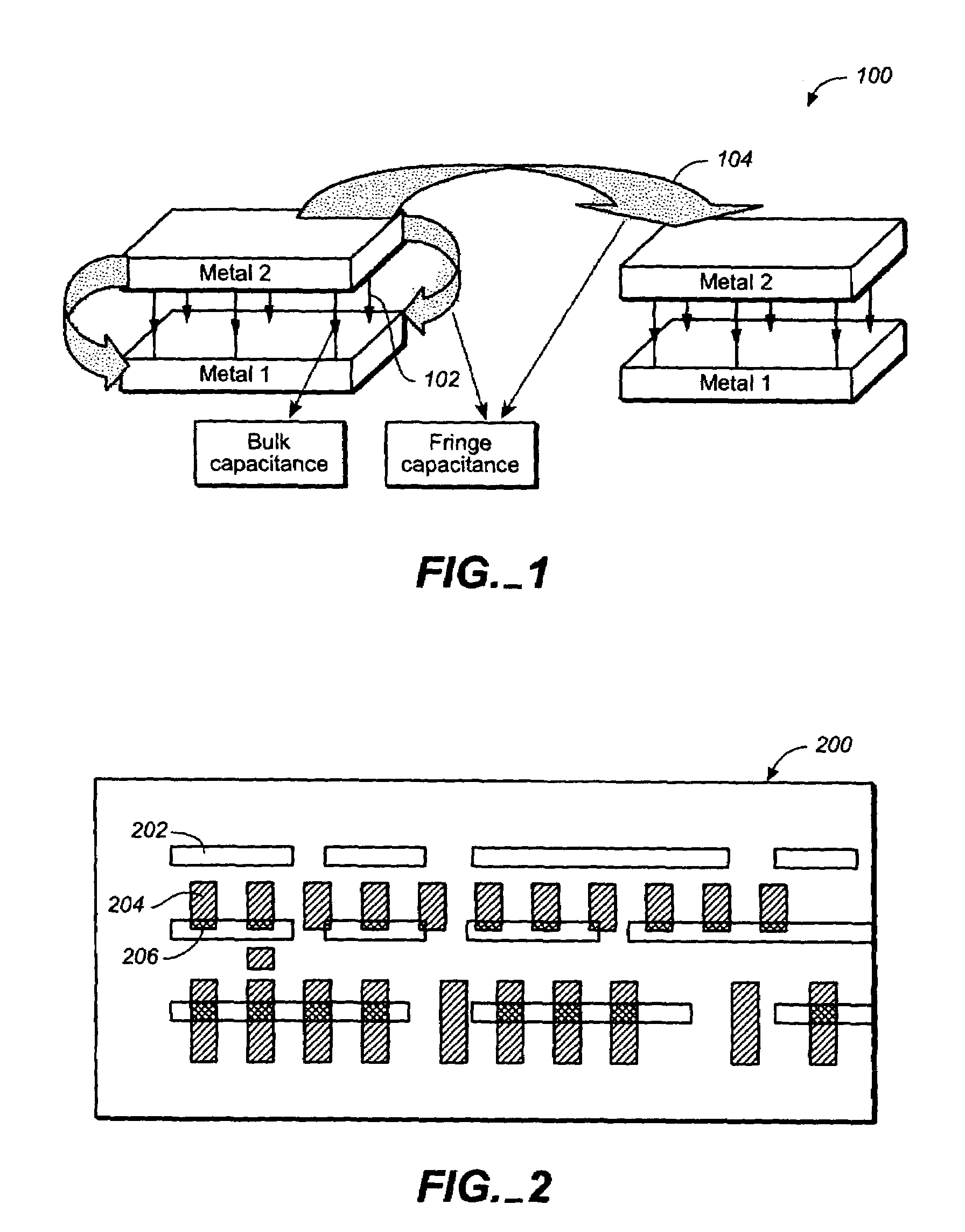
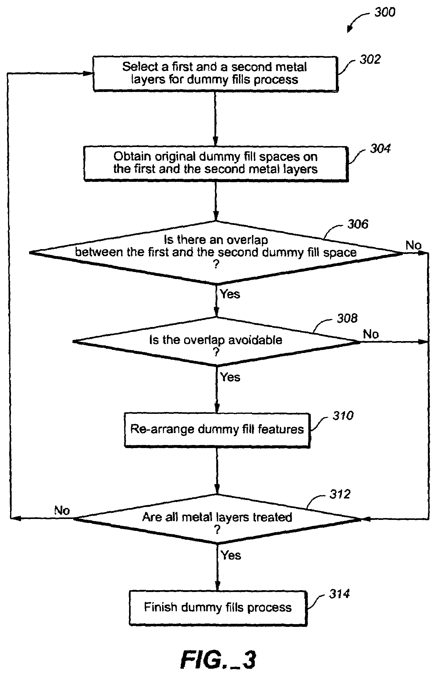
[0021]The present invention is directed to a method and system of intelligent dummy filling placement to reduce inter-layer capacitance caused by overlaps of dummy fills on successive layers. Generally, dummy fill refers to the addition of features to a layout for the purpose of raising the density of specific regions on the layout of the integrated circuit. The method and system treats each consecutive pair of layers together so as to minimize the overlaps of dummy fills between each layer. In particular, dummy fill features on each layer may be placed in a checkerboard pattern to avoid overlaps. As such, the present invention may eliminate large overlap areas of the dummy fills on consecutive layers by utilizing i...


PUM


Abstract

The present invention is directed to a method and system of intelligent dummy filling placement to reduce inter-layer capacitance caused by overlaps of dummy filling area on successive layers. The method and system treats each consecutive pair of layers together so as to minimize dummy filling overlaps between each layer. In particular, dummy fill features on each layer may be placed in a checkerboard pattern to avoid overlaps. As such, the present invention may eliminate large overlap area of the dummy patterns on consecutive layers by utilizing intelligent dummy filling placement.

Description

FIELD OF THE INVENTION[0001]The present invention generally relates to the field of integrated circuit fabrication, and particularly to a method for reducing inter-layer capacitance through dummy fill methodology.BACKGROUND OF THE INVENTION[0002]In any integrated circuit, there is an inevitable capacitance that is introduced from electromagnetic interaction between electrical conductors, such as interconnect layers (metals). There are two components of such capacitance, a bulk (area) component and a fringe (peripheral) component. The bulk component is proportional to the overlap area of interconnect layers and the fringe component depends on the separation and the perimeter of adjacent interconnect layers. Referring now to FIG. 1, the bulk capacitance 102 and the fringe capacitance 104 between Metal 1 and Metal 2 of an exemplary integrated circuit 100 are shown. The bulk capacitance generated due to the overlap of signal carrying lines on Metal 1 and Metal 2 may not be easily avoide...

Claims


Application Information

Patent Timeline
Patent Type & Authority Patents(United States)
IPC IPC(8): H01L21/4763
CPCH01L21/7684H01L23/5222H01L23/522H01L2924/0002H01L2924/00
Inventor TARAVADE, KUNAL N.CALLAN, NEALFILSETH, PAUL G.
Owner BELL SEMICON LLC
Why Eureka
Try Eureka