

Orientation-optimized PFETS in CMOS devices employing dual stress liners
a technology of cmos and pfets, applied in the direction of semiconductor devices, basic electric elements, electrical equipment, etc., can solve the problems of affecting the performance of a particular semiconductor device, the scaling of semiconductor devices, etc., and achieve the effect of increasing the conductivity of an inversion layer
- Summary
- Abstract
- Description
- Claims
- Application Information
AI Technical Summary
Benefits of technology
Problems solved by technology
Method used
Image

Examples
Embodiment Construction
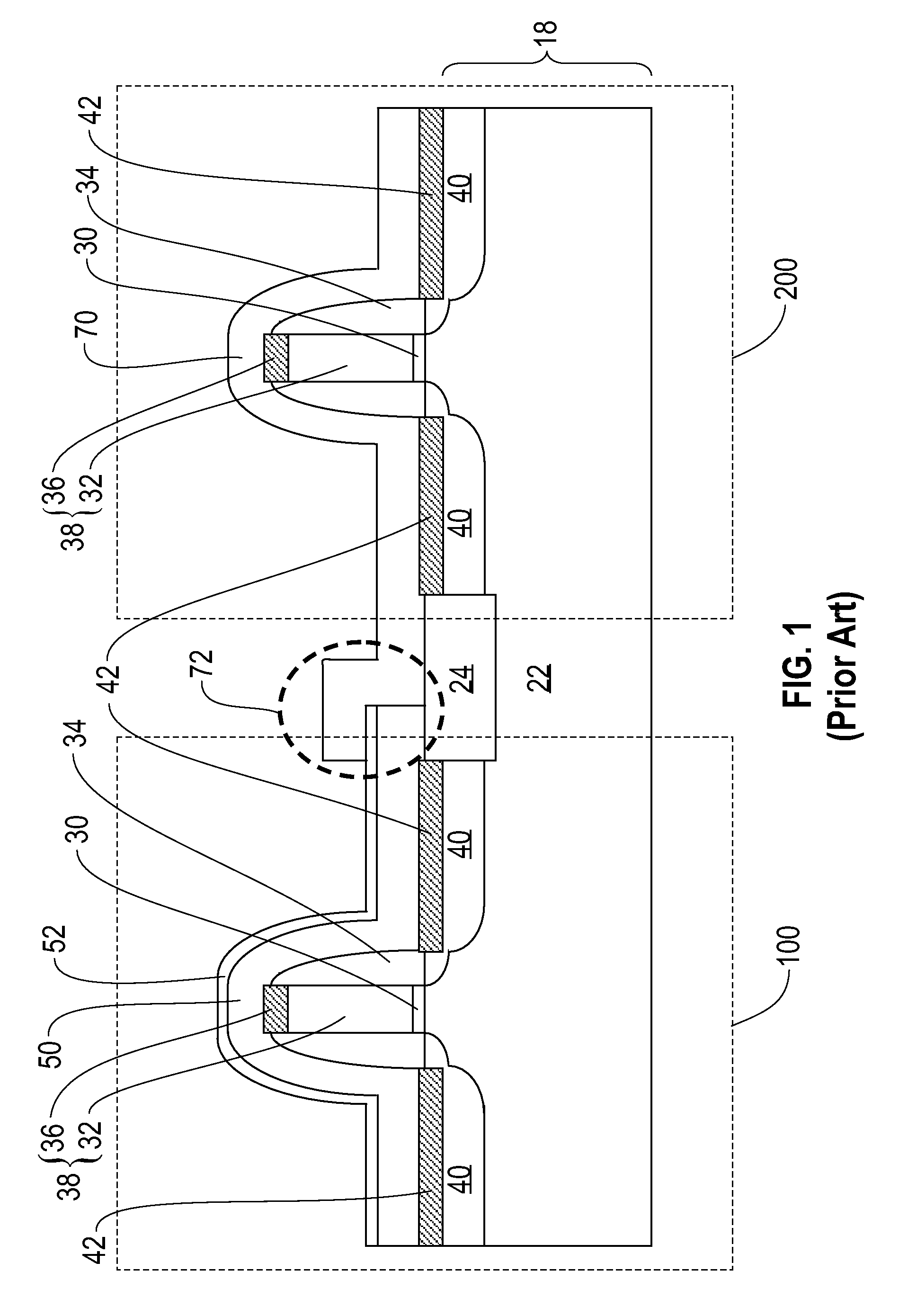
[0064]As stated above, the present invention relates to complementary metal oxide semiconductor (CMOS) transistors with enhanced mobility through biaxial stress generated by dual stress liners, which are now described in detail with accompanying figures. It is noted that like and corresponding elements are referred to by like reference numerals.
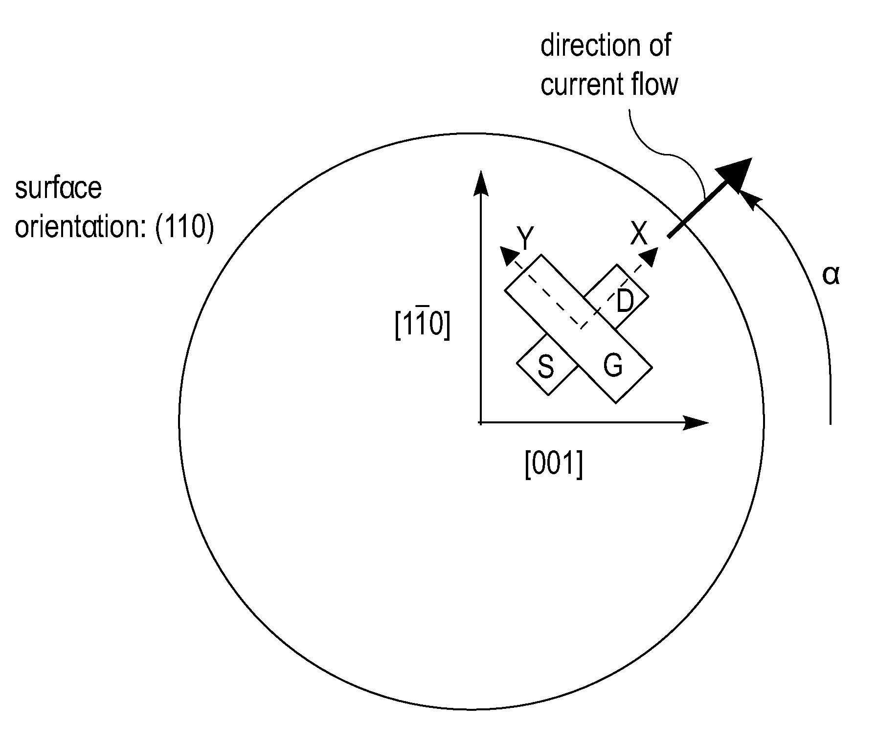
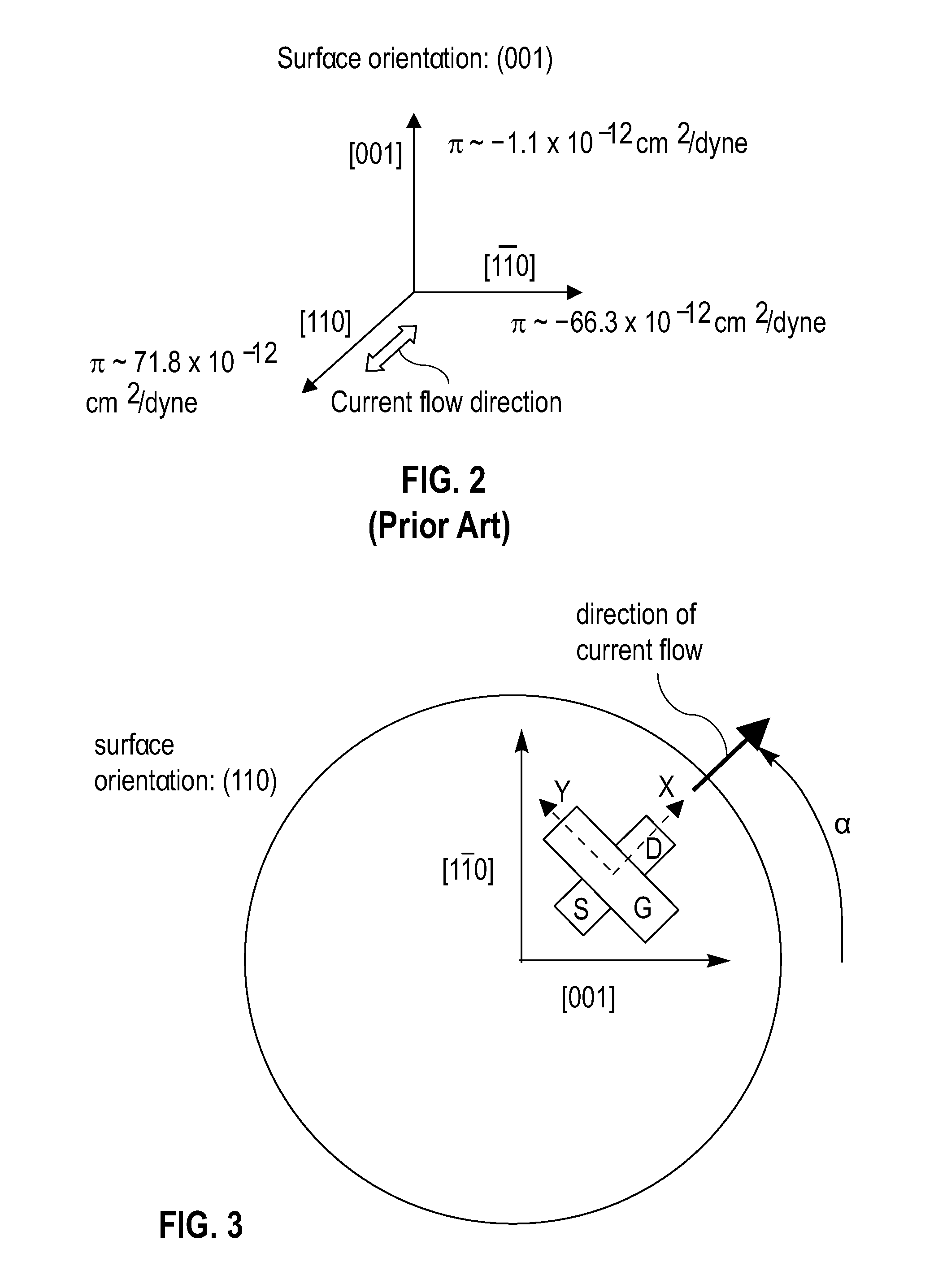
[0065]It is understood that due to inherent symmetry in the crystallographic structure of silicon, the (001) surface orientation may be considered a (100) surface orientation, a (010) surface orientation, a (00 1) surface orientation, etc. in alternate coordinate systems. Likewise, a (110) surface orientation may be considered an (1 1 0) orientation, etc. Such equivalency is implied herein even when not explicitly stated. Further, it is also understood that when different equivalent surface orientations or crystallographic directions are distinguished, for example, between a [110] crystallographic direction and a [1 1 0] crystallographic dire...
PUM
 Abstract
Description
Claims
Application Information