Method and resultant structure for floating body memory on bulk wafer
a floating body memory and bulk wafer technology, applied in the field of integrated circuit memories, can solve the problems of relative high voltage required on the back gate and difficulty in fabricating structures
- Summary
- Abstract
- Description
- Claims
- Application Information
AI Technical Summary
Problems solved by technology
Method used
Image

Examples
Embodiment Construction
[0029]In the following description, a memory and method for fabricating the memory is described. Numerous specific details are set forth, such as specific conductivity types, to provide a thorough understanding of the present invention. It will be apparent to one skilled in the art, that the present invention may be practiced without these specific details. In other instances, well known processing steps have not been described in detail, in order not to unnecessarily obscure the present invention.
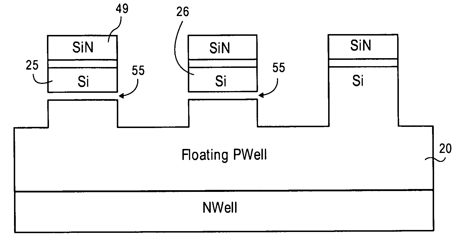
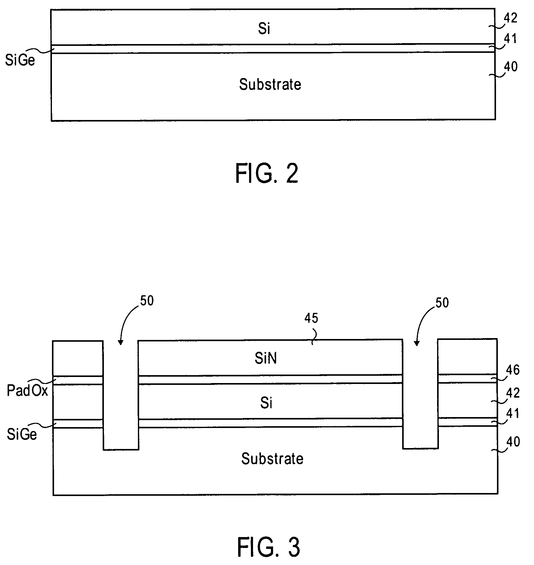
[0030]In the following description, anchors are formed into a substrate and bridges are formed between the anchors. The bridge structure is used to support a first semiconductor layer (e.g. silicon) so that an underlying second semiconductor layer (e.g. SiGe) may be etched away with a selective etchant. The resultant gap is backfilled with an oxide and forms the gate insulation for the back gate of a floating body cell (FBC).
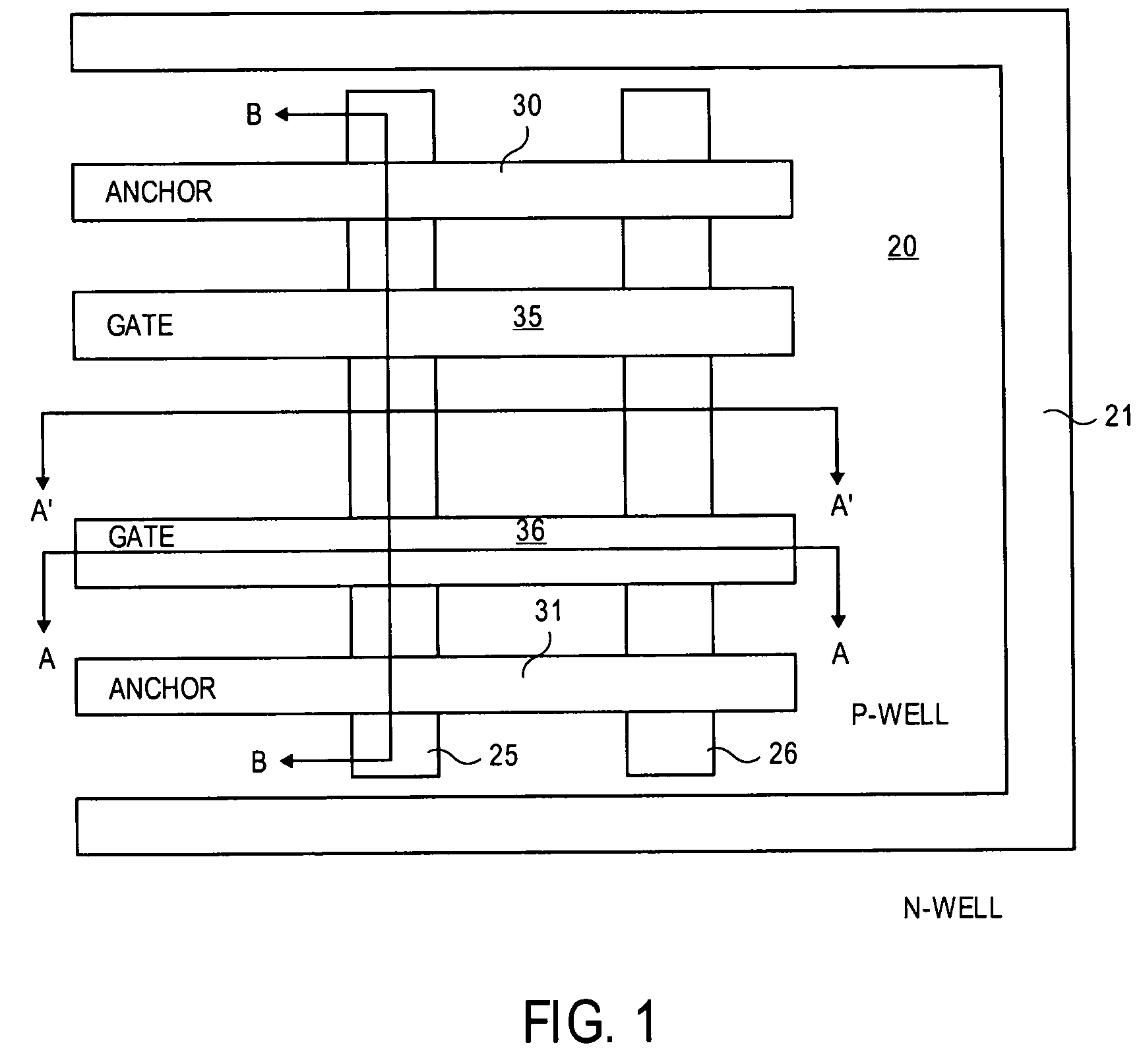
[0031]Referring to FIG. 1, in one embodiment the FBCs are formed ...
PUM
| Property | Measurement | Unit |
|---|---|---|
| charge | aaaaa | aaaaa |
| voltage | aaaaa | aaaaa |
| thick | aaaaa | aaaaa |
Abstract
Description
Claims
Application Information
 - R&D Engineer
- R&D Manager
- IP Professional
- Industry Leading Data Capabilities
- Powerful AI technology
- Patent DNA Extraction
Browse by: Latest US Patents, China's latest patents, Technical Efficacy Thesaurus, Application Domain, Technology Topic.
© 2024 PatSnap. All rights reserved.Legal|Privacy policy|Modern Slavery Act Transparency Statement|Sitemap