Semiconductor memory device comprising floating body memory cells and related methods of operation

a memory cell and semiconductor technology, applied in the direction of information storage, static storage, digital storage, etc., can solve the problems of complex circuit configuration for read operations, erroneous comparison of currents on the bit line and the reference bit line, and read errors

Inactive Publication Date: 2009-08-18
SAMSUNG ELECTRONICS CO LTD
View PDF12 Cites 3 Cited by
  • Summary
  • Abstract
  • Description
  • Claims
  • Application Information

AI Technical Summary

Problems solved by technology

However, charges tend to leak out of the floating body over time and therefore the floating body transistor must be periodically refreshed.
Unfortunately, this variance in current may result in read errors.
Such errors result from erroneous comparisons between currents on the bit line and the reference bit line during data read operations.
In addition to the potential read errors, the conventional semiconductor memory device of FIG. 1 also requires a complicated circuit configuration for read operations.

Method used


Image

  • Semiconductor memory device comprising floating body memory cells and related methods of operation
  • Semiconductor memory device comprising floating body memory cells and related methods of operation
  • Semiconductor memory device comprising floating body memory cells and related methods of operation

Examples


Embodiment Construction

[0032]In general, embodiments of the invention relate to semiconductor memory devices including floating body memory cells and related methods of operation.

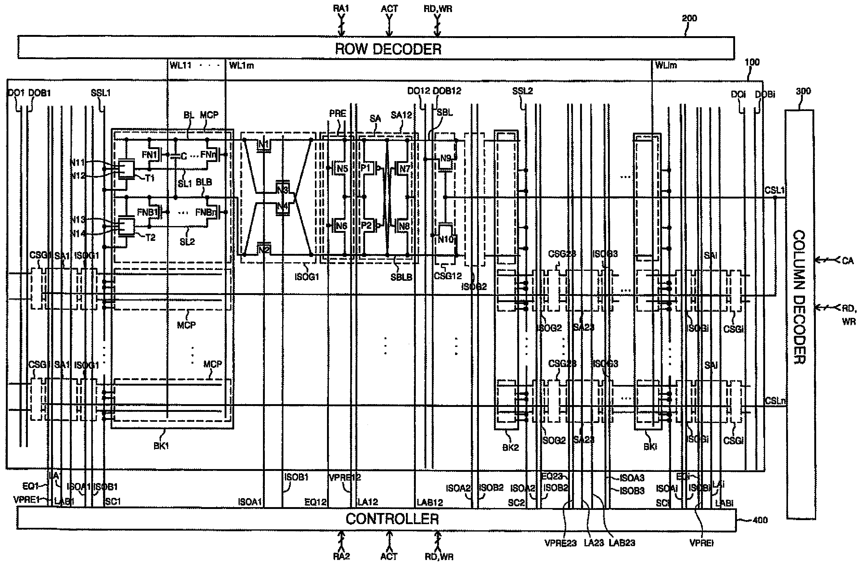
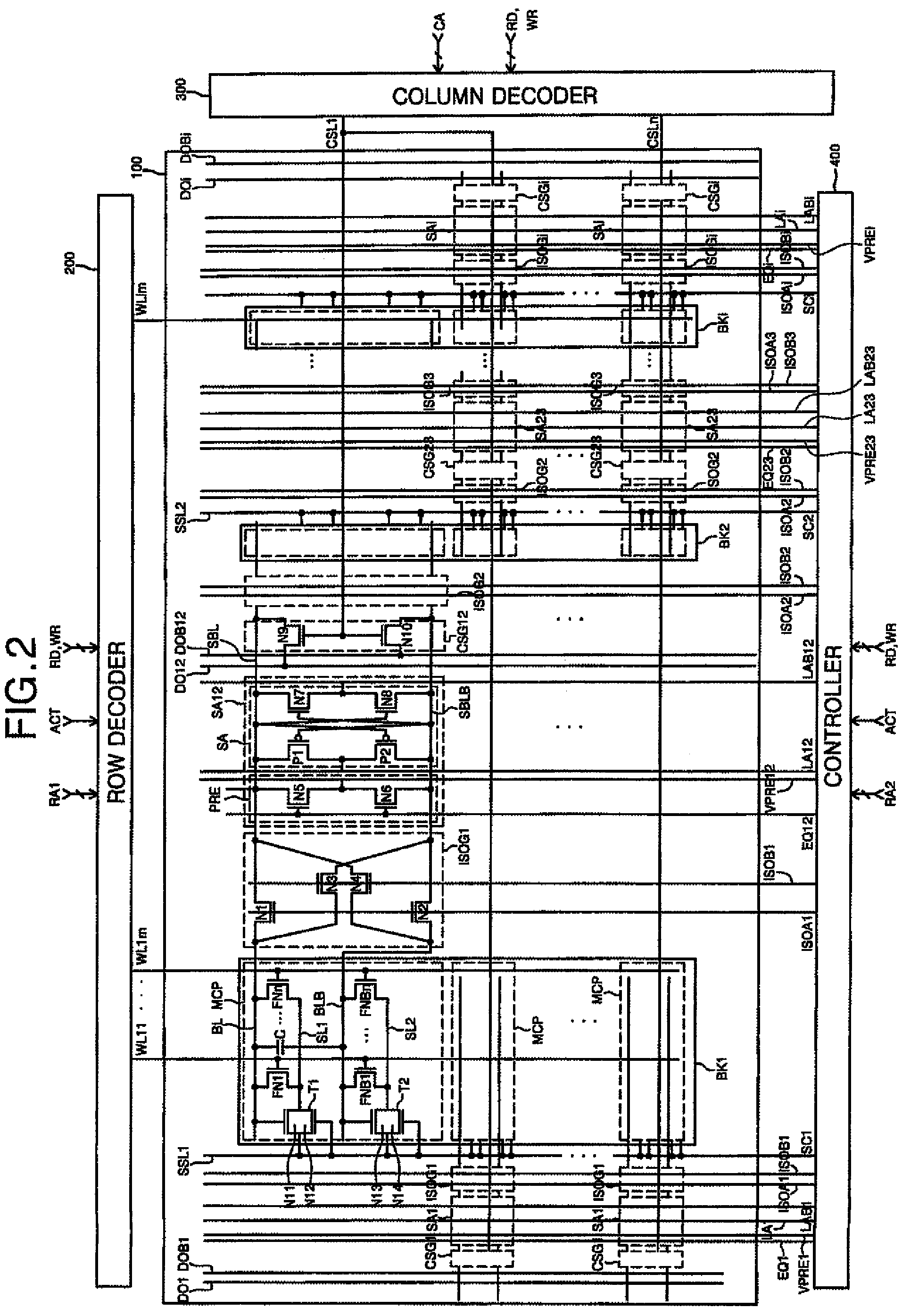
[0033]FIG. 2 is a schematic diagram of a semiconductor memory device according to one embodiment of the invention.

[0034]Referring to FIG. 2, the semiconductor memory device comprises a memory cell array 100, a row decoder 200, a column decoder 300, and a controller 400. Memory cell array 100 comprises “i” memory cell array blocks BK1 through BKi, “i” bit line isolation gates ISOG1 through ISOGi, “i” bit line sense amplifiers SA1, SA12, SA23, . . . , and SAi, and “i” column selection gates CSG1, CSG12, CSG23, . . . , and CSGi. Each of memory cell array blocks BK1 through BKi comprises a plurality of memory pair groups MCP, and each of memory pair groups MCP comprises “n” first memory cells, “n” second memory cells, a first transmission gate T1, and a second transmission gate T2.

[0035]To explain the configuration and operation of m...


PUM


Abstract

A semiconductor device comprising floating body memory cells performs read and write operations by selectively connecting bit lines and inverted bit lines to sense bit lines and inverted sense bit lines.

Description

CROSS-REFERENCE TO RELATED APPLICATIONS[0001]This application claims priority to Korean Patent Application No. 10-2006-0105265, filed Oct. 27, 2006, the disclosure of which is hereby incorporated by reference in its entirety.BACKGROUND OF THE INVENTION[0002]1. Field of the Invention[0003]Embodiments of the present invention relate generally to semiconductor memory devices. More particularly, embodiments of the invention relate to semiconductor memory devices comprising floating body memory cells.[0004]2. Description of Related Art[0005]Researchers continue to seek new ways of increasing the integration density and performance of semiconductor memory cell arrays. One recent proposal for creating smaller memory cell arrays focuses on replacing conventional dynamic random access memory (DRAM) cells with so-called “floating body memory cells”.[0006]In a floating body memory cell, electrical charges are stored in a floating body of a floating body transistor. However, charges tend to lea...

Claims


Application Information

Patent Timeline
Patent Type & Authority Patents(United States)
IPC IPC(8): G11C11/34
CPCG11C11/404G11C11/4091G11C11/4076G11C2211/4016G11C11/4093G11C11/4094G11C11/4097
Inventor KIM, JIN-YOUNGSONG, KI-WHANPARK, DUK-HA
Owner SAMSUNG ELECTRONICS CO LTD
Why Eureka
Try Eureka