Display panel inspection apparatus and method

a technology for display panels and inspection apparatus, applied in the direction of identification means, optically investigating flaws/contamination, instruments, etc., can solve the problems the display panel having defective pixels smaller than a certain proportion of pixels is not treated as a defective product, and the problem of omission of lines is principally a problem, so as to achieve reliable detection of lines, simplify the configuration of the apparatus, and increase the temperature in the interior

Inactive Publication Date: 2009-05-12
FUJITSU LTD
View PDF5 Cites 6 Cited by
  • Summary
  • Abstract
  • Description
  • Claims
  • Application Information

AI Technical Summary

Benefits of technology

[0014]The present invention has been developed in consideration of the above-mentioned problems, and it is therefore an object of the invention to reliably and easily carry out a detection of defective pixels temporarily occurring due to, for example, variations of operating environments such as semi-contact troubles or semi-disconnection troubles.
[0031]The present invention is designed to detect that a pixel is a defective pixel and to hold a result of the detection, which enables a detection of a line omission trouble to be made reliably even in a case in which a line omission trouble stemming from a semi-contact trouble, semi-disconnection trouble or the like occurs temporarily. In addition, the result of the detection of the temporally occurred line omission trouble can be confirmed after the completion of the inspection, which eliminates the need for an inspector to make the confirmation through visual observation during the inspection, thereby reducing the working burden on the inspector. This can improve the detection accuracy of the line omission trouble without imposing a burden on the inspector.
[0032]Moreover, a judgment as to whether a pixel is a defective pixel is made on the basis of the detection state corresponding to the output light of the pixel, thereby reliably and easily specifying the spot where the line omission trouble has occurred.
[0034]In particular, the change of the temperature environment related to the display panel can achieve the reliable detection of a line omission trouble occurring due to the thermal expansion of electrodes, insulating materials and foreign matters stemming from an increase in temperature in the interior of the display panel.
[0035]Furthermore, the arrangement of the plurality of optical detecting units along one side of the display panel enables the detection of the line omission trouble to be made within a short period of time. Still furthermore, the numbers of optical detecting units, judging units and holding units are reducible, which can simplify the apparatus configuration and decrease the manufacturing cost.
[0036]The notification on the output of a detection signal by the judging unit allows easily specifying the spot where a line omission trouble has occurred.

Problems solved by technology

In addition, dot omission troubles due to the appearance of defective pixels in units of pixel and line omission troubles due to the continuous appearance of defective pixels in the form of a line are commonly known as such defective pixels of a display panel.
If a display panel contains defective pixels, the defective pixels cause defects such as difficulty of normal display and display of color different from intended color and, in this manufacturing line, a display panel containing, for example, a certain proportion of defective pixels is handled as a defective product.
Such a very small number of defective pixels sprinkling in the display panel are not remarkable in use, and there is a tendency that a display panel having defective pixels smaller than a certain proportion of pixels is not handled as a defective product.
Meanwhile, since the line omission troubles are remarkable and frequently unsightly because defective pixels appear continuously in a display panel, it is preferred to detect the line omission troubles more effectively in comparison with the dot omission troubles.
Incidentally, such line omission troubles occur principally because foreign matters get mixed between electrodes of a display panel.
Moreover, the line omission trouble of the display panel also occurs due to, for example, the thermal expansion of electrodes, insulating materials and foreign matters getting mixed into the display panel stemming from an increase in temperature in the interior of the display panel, short circuits (semi-contact troubles) between electrodes arising in a case in which the display panel vibrates to move foreign matters therein, or disconnection or breaks (semi-disconnection troubles) of electrode lines and, in many cases, for example, the semi-contact troubles or semi-disconnection troubles occur temporarily (in an instant) because of being involved in variations of operating environment on the display panel such as variations in temperature in the interior of the display panel and vibrations of the display panel itself.
There is a problem which arises with the conventional technique, however, in that difficulty is experienced in detecting the line omission troubles occurring temporarily.
For example, the technique of the above-mentioned Patent Document 1 is made to only once pick up an image of the display screen and, hence, the non-occurrence of a semi-contact trouble or semi-disconnection trouble at the image pickup makes it difficult to detect these troubles, which can cause a line omission trouble to occur during use afterwards even in a case in which no line omission trouble is detected by the inspection conducted when the display panel is put on the market from the factory.
In addition, in the case of the technique disclosed in the above-mentioned Patent Document 1, if the image pickup of the display screen is made more than once, the inspection time to be taken for each display panel lengthens, which leads to incurring an increase in operator's burden or manufacturing cost.

Method used


Image

  • Display panel inspection apparatus and method
  • Display panel inspection apparatus and method
  • Display panel inspection apparatus and method

Examples


Embodiment Construction

[0045]Embodiments of the present invention will be described hereinbelow with reference to the drawings.

[0046][1] Description of Embodiment of the Present Invention

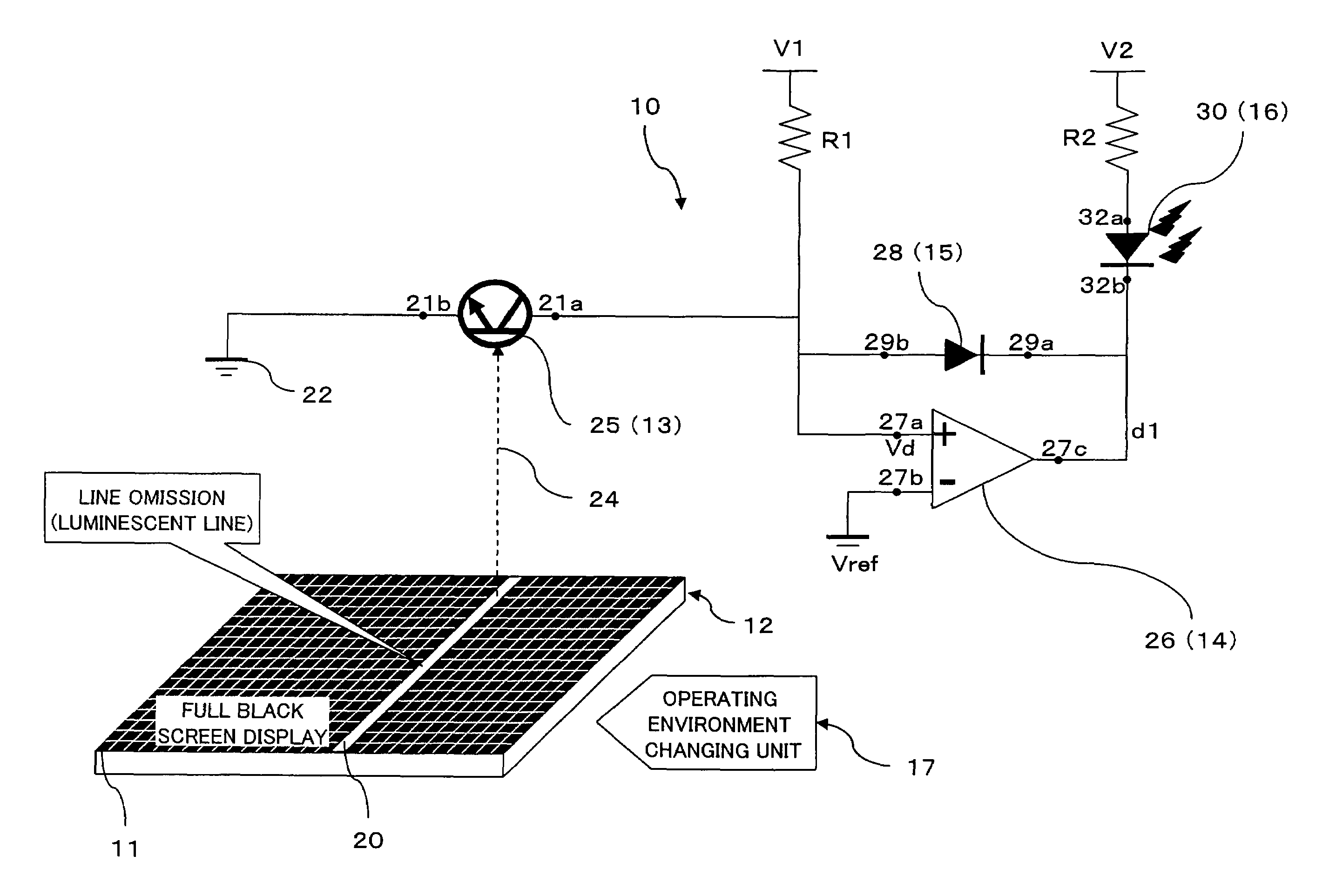
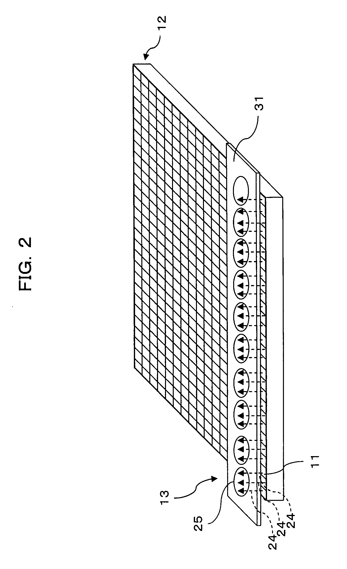
[0047]FIG. 1 illustratively shows an example of a configuration in a case in which a luminescent line is detected as a line omission trouble in a display panel inspection apparatus according to an embodiment of the present invention, FIG. 2 is an illustration useful for explaining an example of a disposition state in an optical detecting unit thereof, and FIG. 3 is an illustration useful for explaining a connection state from an optical detecting unit to a notifying unit therein.

[0048]As shown in FIG. 1, a display panel inspection apparatus 10 according to this embodiment is an apparatus for inspecting a line omission trouble in a rectangular LCD (Liquid Crystal Display; display panel) 12 composed of a plurality of pixels 11 and is configured as an electric circuit including an optical detecting element (detecting unit, o...


PUM

PropertyMeasurementUnit
temperatureaaaaaaaaaa
luminanceaaaaaaaaaa
thermal expansionaaaaaaaaaa

Abstract

The present invention relates to a display panel inspection apparatus for inspecting a display panel composed of a plurality of pixels. The display panel inspection apparatus comprises a detecting unit detecting whether or not each of the pixels is a defective pixel and a holding unit holding a result of the detection by the detecting unit, thereby enabling reliable and easy detection of a defective pixel occurring temporarily due to variations of operation environment such as semi-contact trouble or semi-disconnection trouble, and others.

Description

BACKGROUND OF THE INVENTION[0001]1) Field of the Invention[0002]The present invention relates to a display panel inspection apparatus and method suitable for use in detection of line omission troubles in a display panel such as LCD (Liquid Crystal Display).[0003]2) Description of the Related Art[0004]In general, it is known that a display panel such as LCD (Liquid Crystal Display) sometimes contains defective pixels which do not fulfill their intended function.[0005]In addition, dot omission troubles due to the appearance of defective pixels in units of pixel and line omission troubles due to the continuous appearance of defective pixels in the form of a line are commonly known as such defective pixels of a display panel.[0006]If a display panel contains defective pixels, the defective pixels cause defects such as difficulty of normal display and display of color different from intended color and, in this manufacturing line, a display panel containing, for example, a certain proport...

Claims


Application Information

Patent Timeline
Patent Type & Authority Patents(United States)
IPC IPC(8): G01N21/00
CPCG01N21/95G01N2021/9513G02F1/13G09F9/00
Inventor HACHISUKA, SEIJI
Owner FUJITSU LTD
Why Eureka
Try Eureka