Method of manufacturing electronic circuit device

a manufacturing method and electronic circuit technology, applied in the direction of semiconductor devices, semiconductor/solid-state device details, electrical apparatus, etc., can solve the problems of low patternability of solder resists and unsuitable for high-precision drawing, and achieve low free energy, low solder wettability, and high free energy

Inactive Publication Date: 2009-05-26
RENESAS ELECTRONICS CORP
View PDF8 Cites 8 Cited by
  • Summary
  • Abstract
  • Description
  • Claims
  • Application Information

AI Technical Summary

Benefits of technology

[0009]This method includes preparing the interconnect substrate in which a metal material (first metal material) having relatively high free energy for forming an oxide is exposed in the surface of the electrode pad, while another metal material (second metal material) having relatively low free energy is exposed in the surface of the interconnect. Accordingly, the surface of the interconnect of the interconnect substrate is more susceptible to oxidation than the surface of the electrode pad. Generally a metal oxide layer has lower solder-wettability than the metal, and hence the solder-wettability of the interconnect region becomes lower than that of the electrode pad region when the metal oxide layer is formed on the surface of the interconnect. Accordingly, the solder is prevented from flowing into the interconnect region from the electrode pad region, when connecting the solder electrode of the electronic circuit chip to the electrode pad. The foregoing method, therefore, eliminates the need to employ an interconnect substrate in which a solder resist is provided on the interconnect for preventing the solder from flowing over the interconnect. Consequently, unlike the electronic circuit device shown in FIG. 10, the restriction by the low patternability of the solder resist is no longer imposed on the connection of the interconnect substrate and the electronic circuit chip in a finer pitch.
[0010]Further, since the solder electrode is melted when connected to the electrode pad, the use of the flux is no longer necessary for connecting the interconnect substrate and the electronic circuit chip. Accordingly, the metal oxide layer formed on the interconnect can be prevented from being removed by the flux. The foregoing manufacturing method, therefore, further assures the prevention of the solder from flowing into the interconnect region.

Problems solved by technology

However, generally the solder resist has low patternability, and is hence not suitable for drawing a highly precise and fine pattern.

Method used


Image

  • Method of manufacturing electronic circuit device
  • Method of manufacturing electronic circuit device
  • Method of manufacturing electronic circuit device

Examples


Embodiment Construction

[0023]The invention will be now described herein with reference to illustrative embodiments. Those skilled in the art will recognize that many alternative embodiments can be accomplished using the teachings of the present invention and that the invention is not limited to the embodiments illustrated for explanatory purposes.

[0024]Hereunder, an exemplary embodiment of a method of manufacturing an electronic circuit device according to the present invention will be described, referring to the accompanying drawings. In all the drawings, same constituents are given the same numerals, and the description thereof will not be repeated.

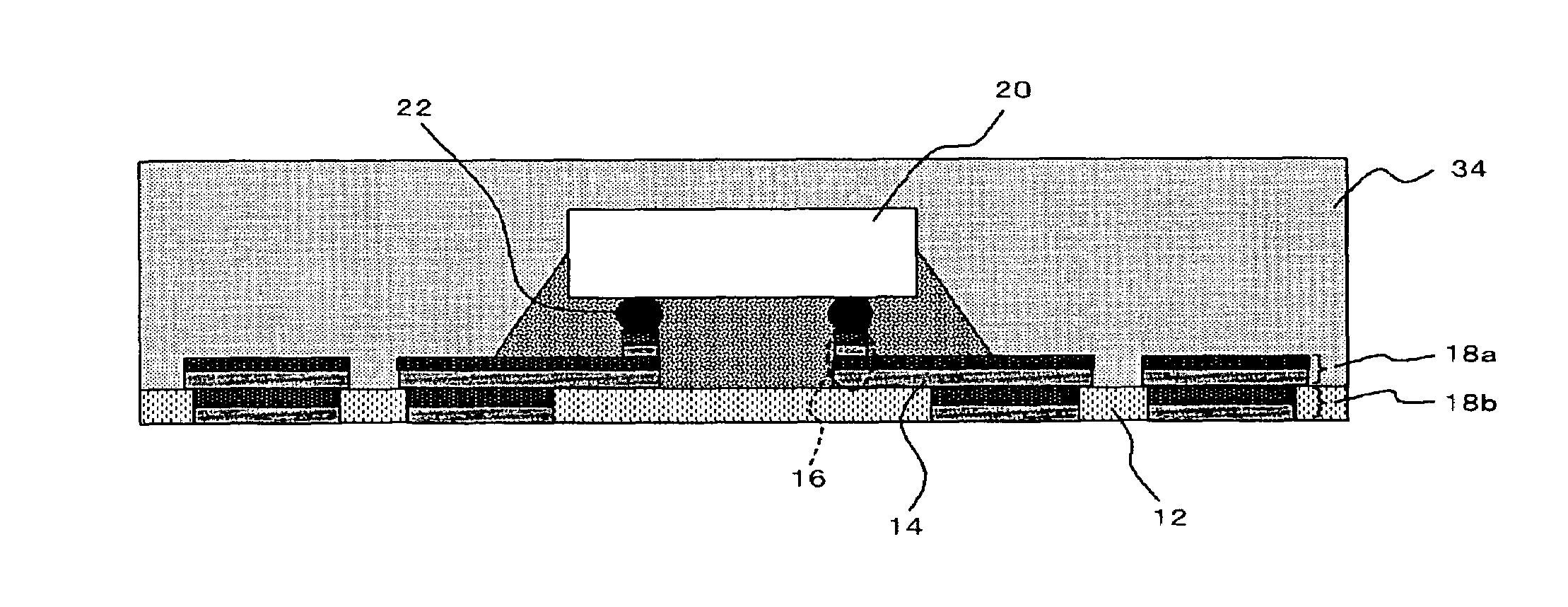
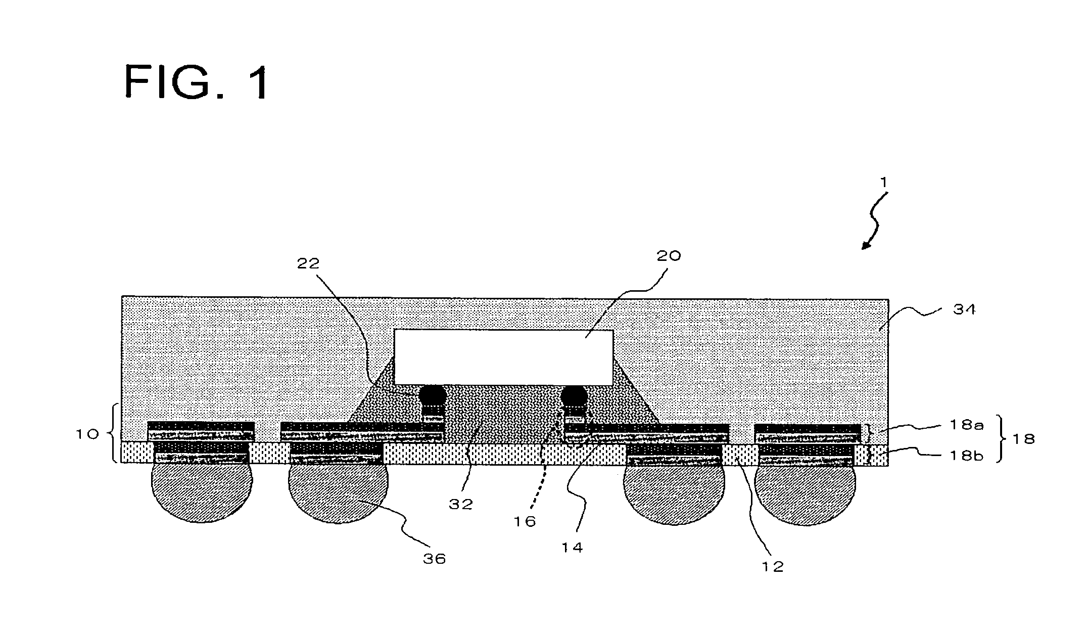
[0025]FIG. 1 is a cross-sectional view showing an electronic circuit device fabricated by a manufacturing method according to an embodiment of the present invention. The electronic circuit device 1 includes an interconnect substrate 10 and an electronic circuit chip 20. The interconnect substrate 10 includes an insulating resin layer 12 (base material), an in...


PUM


Abstract

The method of manufacturing an electronic circuit device according to an embodiment of the present invention includes preparing an interconnect substrate 10 including an interconnect 14 and an electrode pad 16 integrally formed with the interconnect 14; preparing an electronic circuit chip 20 including a solder electrode 22; and melting the solder electrode 22 and connecting it to the electrode pad 16, thus connecting the interconnect substrate 10 and the electronic circuit chip 20. A first metal material, exposed in the surface of the electrode pad 16 opposite to an insulating resin layer 12 and constituting the electrode pad 16, has higher free energy for forming an oxide than a second metal material exposed in the surface of the interconnect 14 opposite to the insulating resin layer 12 and constituting the interconnect 14.

Description

[0001]This application is based on Japanese patent application No. 2005-294713, the content of which is incorporated hereinto by reference.BACKGROUND[0002]1. Technical Field[0003]The present invention relates to a method of manufacturing an electronic circuit device.[0004]2. Related Art[0005]A conventional method of manufacturing an electronic circuit device can be found, for example, in Japanese Laid-open patent publication No. H05-144816. FIG. 10 is a cross-sectional view showing an electronic circuit device manufactured by the method disclosed therein. The electronic circuit device shown in FIG. 10 is obtained by connecting an interconnect substrate 100 and a semiconductor chip 110. In the interconnect substrate 100, an interconnect 103 and an electrode pad 104 are provided on a base material 101, via an adhesive 102. The interconnect 103 and the electrode pad 104 constitute an integral conductor pattern. On the interconnect 103, a solder resist 105 is provided to prevent solder ...

Claims


Application Information

Patent Timeline
Patent Type & Authority Patents(United States)
IPC IPC(8): H01L21/44H01L21/00H01L21/4763
CPCH01L21/563H01L21/6835H01L23/3128H01L24/28H01L24/81H01L2224/73204H01L2224/32225H01L2224/16225H01L2924/014H01L2924/01024H01L2924/01006H01L2924/19043H01L2924/19041H01L2924/15311H01L2924/01079H01L2924/01078H01L2924/0105H01L2924/01047H01L2221/68345H01L2224/73203H01L2224/75252H01L2224/81054H01L2224/81193H01L2224/81203H01L2224/81801H01L2224/83102H01L2224/92125H01L2924/01002H01L2924/01005H01L2924/01029H01L2924/01033H01L2924/01046H01L2924/00H01L2924/181H01L2924/00012
Inventor KURITA, YOICHIROSOEJIMA, KOJIKAWANO, MASAYA
Owner RENESAS ELECTRONICS CORP
Why Eureka
Try Eureka