Liquid crystal display device

a display device and liquid crystal technology, applied in non-linear optics, instruments, optics, etc., can solve problems such as the inability to propagate the tilt direction, and achieve the effect of improving the alignment and improving the display quality

Active Publication Date: 2009-06-30
SHARP KK
View PDF14 Cites 8 Cited by
  • Summary
  • Abstract
  • Description
  • Claims
  • Application Information

AI Technical Summary

Benefits of technology

[0021]It is an object of the invention to provide in a liquid crystal display device in which a second TFT 60 is provided between a sub-pixel directly connected to a TFT and a floating sub-pixel in order to prevent image sticking in an MVA type with a half tone method using a floating sub-pixel, the alignment is improved and display quality is improved. FIG. 1 shows a principle structural view. There are provided a first and a second substrates disposed to be opposite to each other, a liquid crystal sealed between the first and the second substrates, a gate bus line 12 and a data bus line 14 formed on the first substrate, a first TFT 20 connected to the gate bus line 12 and the data bus line 14, a plurality of sub-pixel electrodes formed in a pixel region defined by the gate bus line 12 and the data bus line 14, and a control electrode which is capacitance coupled to at least one of the plurality of sub-pixel electrodes and to which a displayed voltage is applied from the data bus line 14 through the first TFT 20. Further, there is provided a second TFT 60 which is driven by a signal flowing through a gate bus line different from the gate bus line 12 to which the TFT 20 is connected. Here, the second TFT 60 causes a short circuit between “the sub-pixel electrode capacitance-coupled to the control electrode” and “an auxiliary capacitance bus line 18a kept at a specific potential and constituting an auxiliary capacitance between itself and the control electrode” or causes a short circuit between “the sub-pixel electrode capacitance-coupled to the control electrode” and “the sub-pixel electrode connected to the first TFT 20”. The control electrode of a pixel adjacent to a corner portion of each pixel, which has been a cause of alignment disturbance of liquid crystal molecules since the propagation distance is long, is extended and is disposed.
[0023]A first function is to shorten a distance in which the tilt of liquid crystal molecules is propagated and to prevent the liquid crystal molecules from being tilted in a direction other than a specified direction. In the conventional structure shown in FIG. 3, although the minute slit 46a exists, since the distance in which the tilt of liquid crystal molecules is propagated is long, the alignment is disturbed. On the other hand, in this embodiment, the slit 48 is formed, so that the distance in which the tilt of liquid crystal molecules is propagated becomes short, the liquid crystal molecules are not tilted in a direction other than the specified direction, and the alignment becomes stable.
[0024]A second function is obtained by a lateral electric field between the alignment control electrode 65 and the pixel electrode 17a. When dot inversion drive is performed, in case a common electrode 41 has a reference potential, potentials of the alignment control electrode 65 and the pixel electrode 17a are in a relation of reverse polarity. Accordingly, a lateral electrode field having a potential difference at least twice as high as the voltage for black is always generated between the alignment control electrode 65 and the pixel electrode 17a. By this lateral electric field, the liquid crystal molecules on the slit 48 keep a state where they stand in the vertical direction to the substrate. Even if liquid crystal molecules are tilted in a direction different from the specified direction, the propagation thereof does not overpass the slit 48. In order to enable the tilt of the liquid crystal molecules to be propagated, a vertical electric field must be generated between the common electrode 41 and the pixel electrodes 16 and 17 so that a force to tilt the liquid crystal molecules is applied. However, since the force to tile is not exerted on the liquid crystal molecules in the lateral electric field, the liquid crystal molecules are not tilted, and accordingly, the tilt direction can not be propagated. Especially, since the gate bus line has generally a potential lower than the pixel electrode by several volts to ten and several volts, in the vicinity of the gate bus line, the lateral electric field is generated in a direction different from the specified alignment direction, and the liquid crystal molecules are tilted in the direction different from the specified direction. However, the propagation is blocked by the slit 48, and the alignment of the liquid crystal molecules on the pixel electrode 17a is stabilized.

Problems solved by technology

However, since the force to tile is not exerted on the liquid crystal molecules in the lateral electric field, the liquid crystal molecules are not tilted, and accordingly, the tilt direction can not be propagated.

Method used


Image

  • Liquid crystal display device
  • Liquid crystal display device
  • Liquid crystal display device

Examples


first embodiment

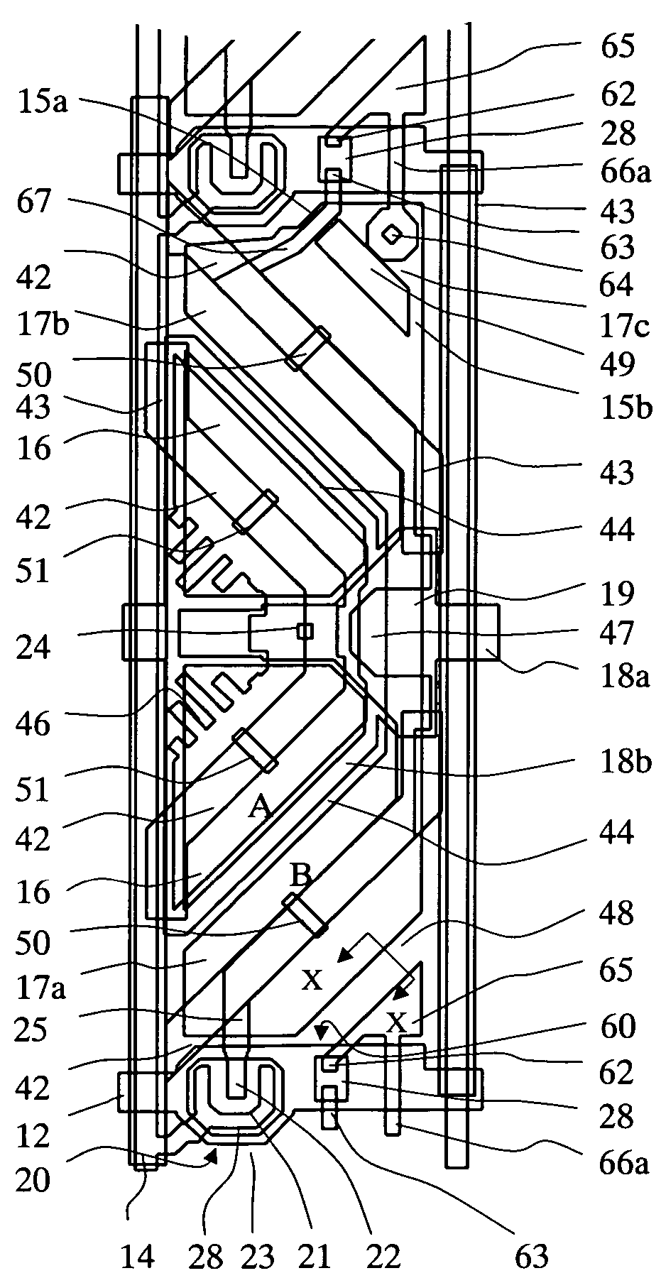
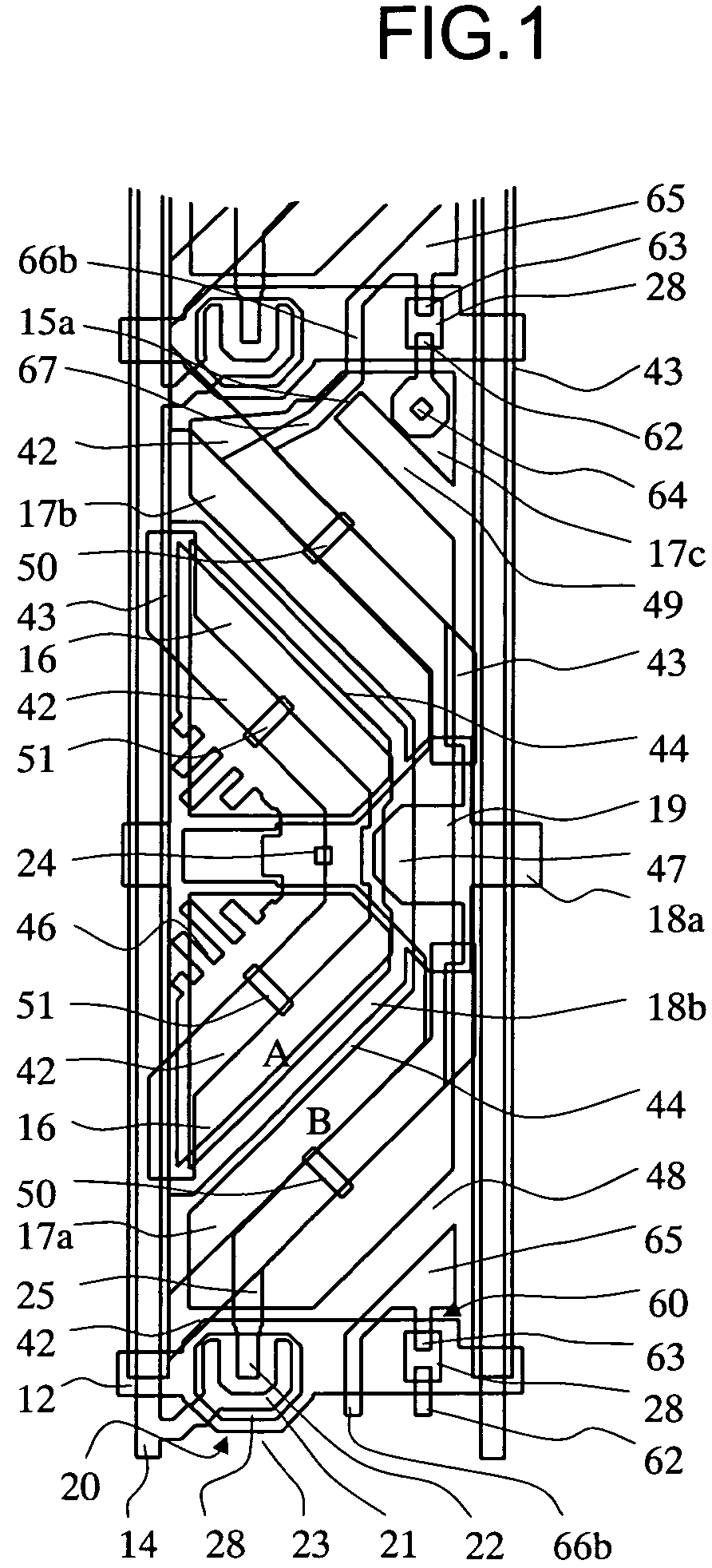
[0036]A liquid crystal display device according to a first embodiment of the invention will be described with reference to FIGS. 4, 5 and 7. FIG. 4 shows the rough structure of the liquid crystal display device of this embodiment. As shown in FIG. 4, the liquid crystal display device includes a TFT substrate 2 having a gate bus line 12 and a drain bus line 14 formed to intersect with each other through an insulating film, a TFT formed for each pixel and a pixel electrode. Besides, the liquid crystal display device includes an opposite substrate 4 which is disposed to be opposite to the TFT substrate 2 and on which a CF and a common electrode are formed, and a liquid crystal 6 (not shown in FIG. 4) sealed between both the substrates 2 and 4 and having, for example, a negative dielectric anisotropy. Vertical alignment films (not shown) to cause the liquid crystal 6 to be vertically aligned are formed on interfaces between the liquid crystal 6 and the TFT substrate 2 and between the li...

second embodiment

[0053]Next, a liquid crystal display device of a second embodiment of the invention will be described with reference to FIG. 6. FIG. 6 shows a structure of one pixel and part of upper and lower pixels adjacent thereto in the liquid crystal display device of this embodiment. As shown in FIG. 6, in this embodiment, differently from the first embodiment (see FIG. 4), a re-extension part 66b of an extension part 67 of a control capacitance electrode 25 strides across a gate bus line 12, and is electrically connected to an alignment control electrode 65 of an adjacent pixel. The alignment control electrode 65 is electrically connected to a drain electrode 63 of a second TFT 60. On the other hand, a contact hole 64 is electrically connected to a source electrode 62 of the second TFT 60.

[0054]At the instance when the gate bus line 12 to drive the second TFT 60 comes to have an OFF voltage, potentials of both sub-pixels A and B are decreased by a capacitance between each of the sub-pixels A...

third embodiment

[0056]Next, a liquid crystal display device of a third embodiment of the invention will be described with reference to FIGS. 8 and 9. In this embodiment, differently from the first and the second embodiments, a portion 15b to connect a pixel electrode 17b and a pixel electrode 17c is eliminated, and a slit 49 has such a shape that one side is opened. FIG. 8 is a view in which the vicinity of the slit 49 of FIG. 6 is enlarged and a dark line generated in the vicinity of the slit 49 is schematically shown. FIG. 9 is a view in which the vicinity of the slit 49 of FIG. 1 is enlarged and a dark line generated in the vicinity of the slit 49 is schematically shown. In the pixel electrode shape in which a connection portion 15b shown in FIG. 8 exists, dark lines 71a and 71b undulate and enter the inside of the pixel electrode 16, and a dark region is also generated. However, when there is no connection portion 15b as shown in FIG. 9, shapes of dark lines 71a and 71b become simple shapes alo...


PUM

PropertyMeasurementUnit
widthsaaaaaaaaaa
angleaaaaaaaaaa
widthaaaaaaaaaa

Abstract

In a liquid crystal display device in which in order to prevent image sticking in a half tone type MVA using a floating sub-pixel, a second TFT is provided between a sub-pixel directly connected to a TFT and the floating sub-pixel, its alignment is improved and a display quality is improved. A control capacitance electrode of an adjacent pixel is extended to provide an alignment control electrode in a corner portion of a pixel in which a propagation distance of liquid crystal alignment is long, and the propagation distance of the liquid crystal alignment is shortened, and at the same time, a slit part is formed of electrodes different from each other in voltage polarity to stabilize the alignment.

Description

BACKGROUND OF THE INVENTION[0001]1. Field of the Invention[0002]The present invention relates to a liquid crystal display device including plural sub-pixel electrodes in one pixel region and improved in alignment of liquid crystal molecules, and particularly to a liquid crystal display device in which at least one sub-pixel electrode is capacitance coupled to a control electrode to which a display voltage is applied, and is connected through a second TFT to a sub-pixel electrode directly driven by the control electrode in order to prevent image sticking.[0003]2. Description of the Related Art[0004]As compared with a CRT (Cathode Ray Tube), a liquid crystal display device has merits that it is thin, is lightweight, is driven by a low voltage, and has small electric power consumption. Thus, the liquid crystal display device is used for various electric equipments such as a television, a notebook PC (Personal Computer), a desktop PC, PDA (Personal Digital Assistant) and a cellular phon...

Claims


Application Information

Patent Timeline
Patent Type & Authority Patents(United States)
IPC IPC(8): G02F1/136G02F1/1343
CPCG02F1/1337G02F1/133707G02F1/1343G02F1/1393
Inventor NAKANISHI, YOHEIYOSHIDA, HIDEFUMITASAKA, YASUTOSHI
Owner SHARP KK
Why Eureka
Try Eureka