System and method for reducing pin-count of memory devices, and memory device testers for same

a memory device and pin-count reduction technology, applied in the field of memory devices, can solve problems such as several problems and limitations, and increase the pin-count of integrated circuits

Active Publication Date: 2009-06-30
MICRON TECH INC
View PDF12 Cites 8 Cited by
  • Summary
  • Abstract
  • Description
  • Claims
  • Application Information

AI Technical Summary

Problems solved by technology

These increases in the pin count of integrated circuits can present a variety of problems.
As explained in greater detail below, the need to connect the memory devices 14a,b to the tester 12 in this manner can result in several problems and limitations.

Method used


Image

  • System and method for reducing pin-count of memory devices, and memory device testers for same
  • System and method for reducing pin-count of memory devices, and memory device testers for same
  • System and method for reducing pin-count of memory devices, and memory device testers for same

Examples


Embodiment Construction

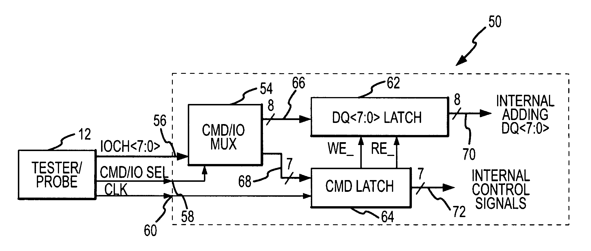
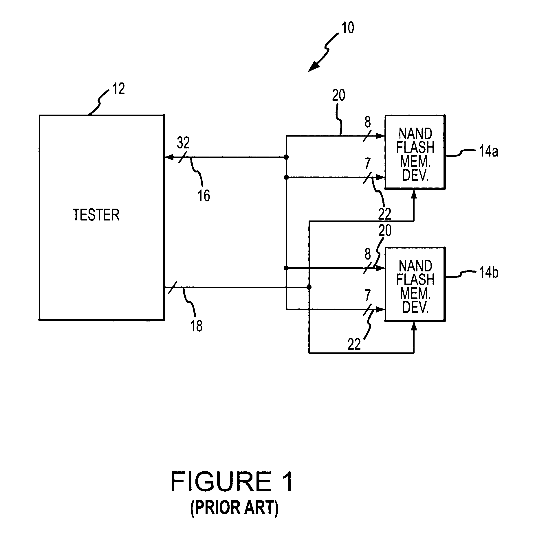
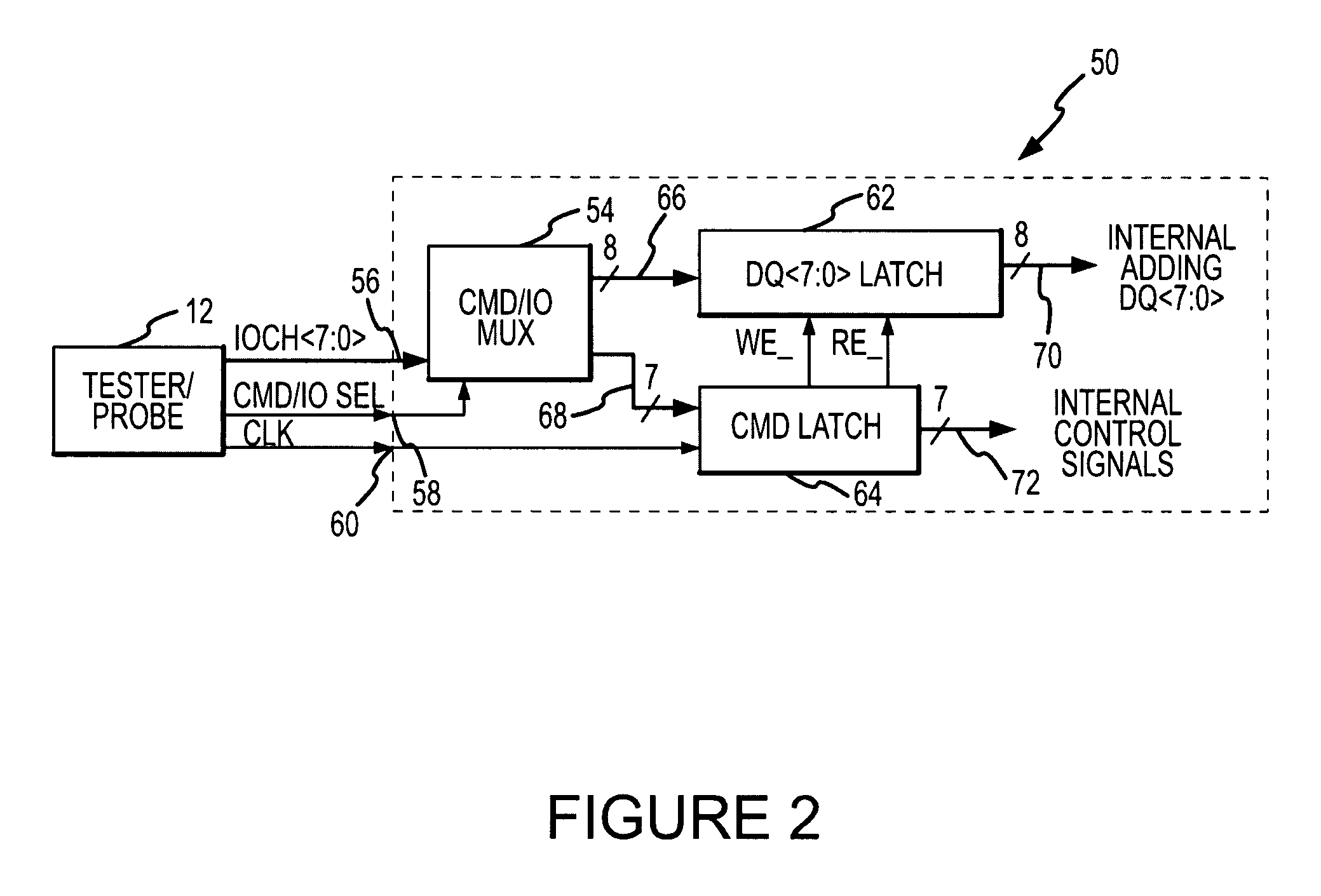
[0012]The prior art tester 12 and the NAND flash memory devices 14a,b shown in FIG. 1 can be connected to each other for testing in a variety of configurations, one of which is shown in Table 1, below:

[0013]

TABLE 1Tester 12Memory Device 14aMemory Device 14bIO-0 IO-0IO-1 IO-1IO-2 IO-2IO-3 IO-3IO-4 IO-4IO-5 IO-5IO-6 IO-6IO-7 IO-7IO-8 ALEIO-9 CL#IO-10CE#IO-11RE#IO-12WE#IO-13PREIO-14WP#IO-15IO-16IO-0IO-17IO-1IO-18IO-2IO-19IO-3IO-20IO-4IO-21IO-5IO-22IO-6IO-23IO-7IO-24ALEIO-25CL#IO-26CE#IO-27RE#IO-28WE#IO-29PREIO-30WP#IO-31

[0014]It will be apparent from Table 1 that the tester 12 can test only two of the NAND flash memory devices 14a,b at the same time. Conventional integrated circuit testers, such as the tester 12, are very expensive. It would therefore be desirable to be able to test more than two of the NAND flash memory devices 14a,b at the same time. For example, if the tester 12 could simultaneously test three of the NAND flash memory devices 14, the capital cost of testing could be...


PUM


Abstract

Methods, memory devices and systems are disclosed. In one embodiment, a non-volatile memory device receives command signals through the same input / output terminals that receive address signals and write data signals and transmit read data signals. The input / output terminals are connected to a multiplexer, which is responsive to a received mode control signal to couple the input / output terminals to either a command bus or an input / output bus. A latch in the memory device latches the command signals when the mode control signal causes the input / output terminals to be coupled to the input / output bus. As a result, the command signals continue to be applied to the command bus. When the mode control signal causes the input / output terminals to be coupled to the input / output bus, write data signals are clocked into the memory device and read data signals are clocked out of the memory device responsive to a received clock signal.

Description

TECHNICAL FIELD[0001]This invention relates generally to memory devices, and, more particularly, to a memory device and method having a reduced pin count, as well as to a memory device tester.BACKGROUND OF THE INVENTION[0002]Integrated circuits, such as memory devices, are housed in a package having externally accessible terminals known as “pins” for coupling power and signals to the integrated circuits and signals from the integrated circuits. The pins are internally connected to bonding pads fabricated with circuitry on a semiconductor substrate. As the level of integration continues to increase, the number of bonding pads and resulting pins in an integrated circuit can correspondingly increase. These increases in the pin count of integrated circuits can present a variety of problems. For example, a high pin count can reduce the ability to test integrated circuits in a cost-efficient manner. This problem is exemplified by a testing system 10 shown in FIG. 1 in which a tester 12 is...

Claims


Application Information

Patent Timeline
Patent Type & Authority Patents(United States)
IPC IPC(8): G11C7/10
CPCG11C5/066G11C29/1201G11C29/48G11C7/10G11C2029/2602
Inventor GATZEMEIER, SCOTTFISTER, WALLACEJOHNSON, ADAMLOUIE, BEN
Owner MICRON TECH INC
Why Eureka
Try Eureka