

Surface-emitting laser diode having reduced device resistance and capable of performing high output operation, surface-emitting laser diode array, electrophotographic system, surface-emitting laser diode module, optical telecommunication system, optical interconnection system using the surface-emitting laser diode, and method of fabricating the surface-emitting laser diode
a laser diode and laser diode technology, applied in the field of surface-emitting laser diodes, can solve the problems of increasing the resistance, increasing the amount of confined light, and difficult to achieve high output, so as to achieve the effect of preventing the increase of the device resistan
- Summary
- Abstract
- Description
- Claims
- Application Information
AI Technical Summary
Benefits of technology
Problems solved by technology
Method used
Image

Examples
eighth embodiment
(Eighth Embodiment)
[0199]An eighth embodiment of the present invention is a surface-emitting laser diode that has the same structure as one of the surface-emitting laser diodes of the first through seventh embodiments, except that at least one of the distributed Bragg reflectors is a n-type semiconductor distributed Bragg reflector, and that a tunnel junction is provided between the n-type semiconductor distributed Bragg reflector and the active layer.
[0200]With this structure of the eighth embodiment that employs an n-type semiconductor distributed Bragg reflector with a small absorption loss, instead of a p-type semiconductor distributed Bragg reflector, a highly efficient surface-emitting laser diode can be obtained.
ninth embodiment
(Ninth Embodiment)
[0201]A ninth embodiment of the present invention is a surface-emitting laser diode that has the same structure as one of the surface-emitting laser diodes of the first through eighth embodiments, except that at least one of the distributed Bragg reflectors is a non-doped semiconductor distributed Bragg reflector or a Bragg reflector partially including a region formed by a non-doped semiconductor distributed Bragg reflector, and that an electrode for confining carriers is provided on a semiconductor layer between the active layer and the non-doped semiconductor distributed Bragg reflector or the region formed by a non-doped semiconductor Bragg reflector.
[0202]With this structure of the ninth embodiment that employs a non-doped semiconductor distributed Bragg reflector with a small absorption loss, a highly efficient surface-emitting laser diode can be obtained.
tenth embodiment
(Tenth Embodiment)
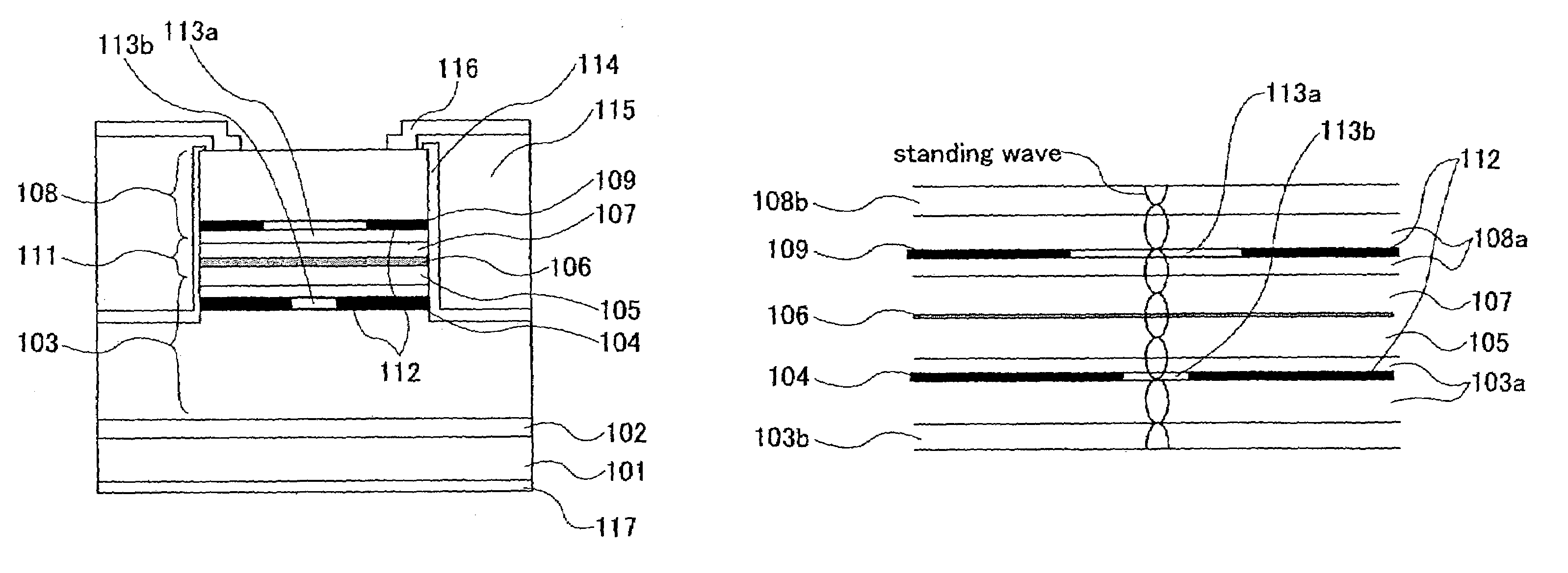
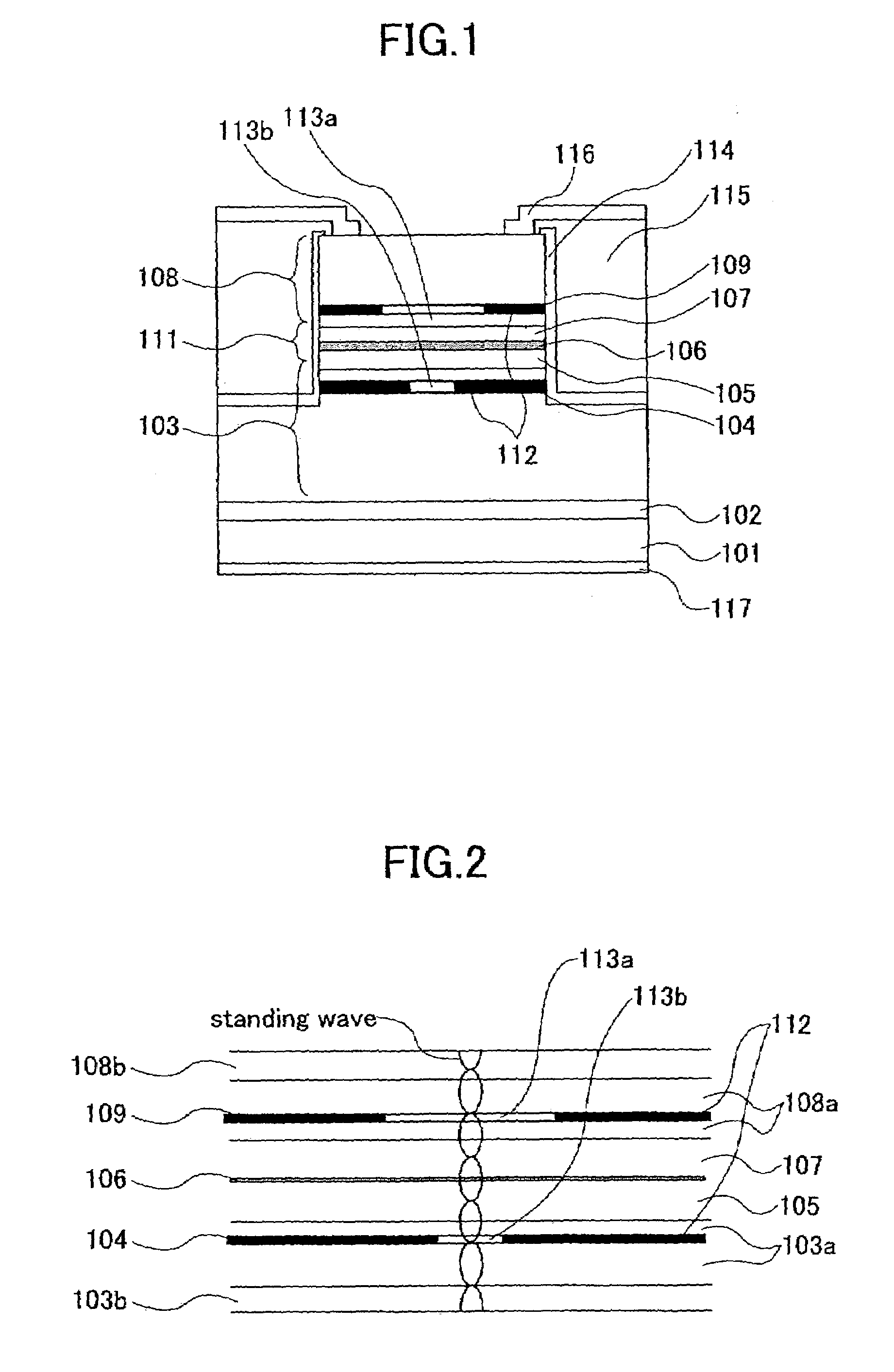
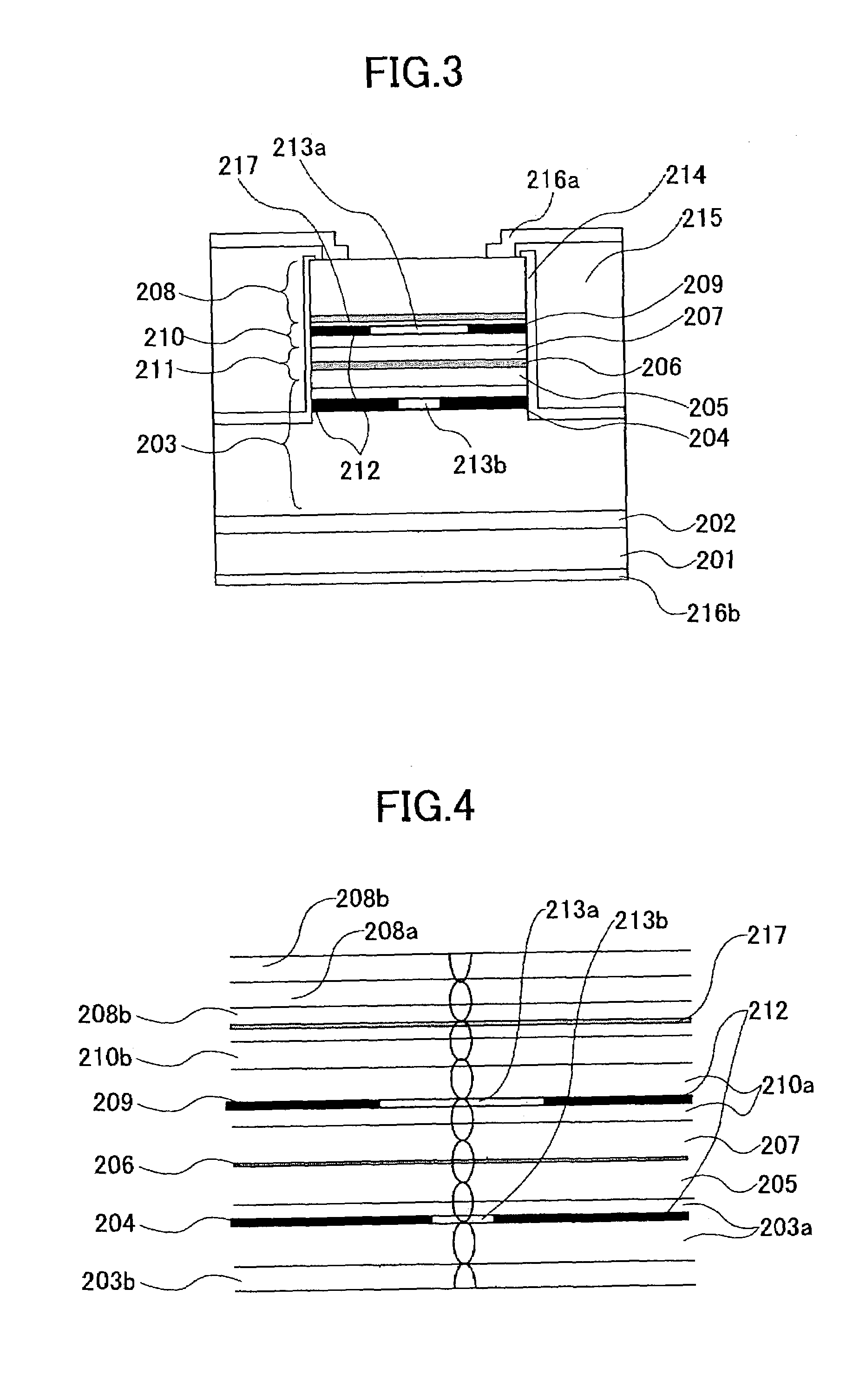
[0203]A tenth embodiment of the present invention is a surface-emitting laser diode having the same structure as one of the surface-emitting laser diodes of the first through ninth embodiments, except that the hole restricting structure in the hole passage is provided at a location corresponding to an antinode of the standing wave of oscillating light.
[0204]With this structure of the tenth embodiment, the optical mode control structure formed by the selective oxidation structure provided at a location corresponding to an antinode of the standing wave of oscillating light can retrain high-order transverse-mode oscillation with greater effect.
PUM
 Abstract
Description
Claims
Application Information