This helps you quickly interpret patents by identifying the three key elements:
Problems solved by technology
Method used
Benefits of technology
Benefits of technology
[0013]The semiconductor device according to the present invention is provided with a trench in the covering film so that the contact area between the covering film and the sealing film is increased and therefore it becomes difficult for the sealing film to become detached.
[0015]The manufacturing method according to the present invention comprises a process for providing a trench in the covering film so that the contact area between the covering film and the sealing film is made larger and therefore it becomes possible to manufacture a semiconductor device in which it is difficult for the sealing film to become detached.
Problems solved by technology
However, in contemporary semiconductor devices there tends to be a large number of external terminals.
In addition, in contemporary semiconductor devices there has been a tendency for the chips to become smaller in size.
In order to maintain the reliability of semiconductor devices, it is necessary to make it difficult for the sealing film to become detached from the surface of the chip.
Method used
Image
Click on the blue label to locate the original text in one second.
Reading with bidirectional positioning of images and text.
Examples
first embodiment
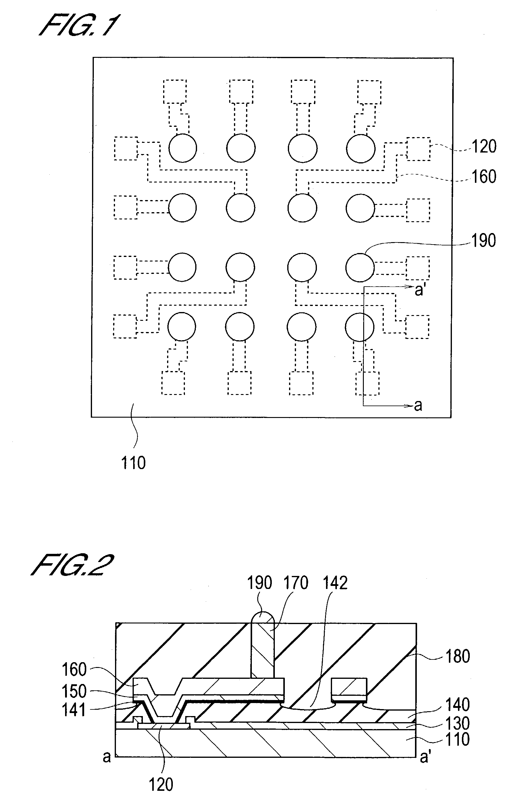
[0027]Firstly, a first embodiment of the invention will be explained with reference to FIGS. 1 to 6.
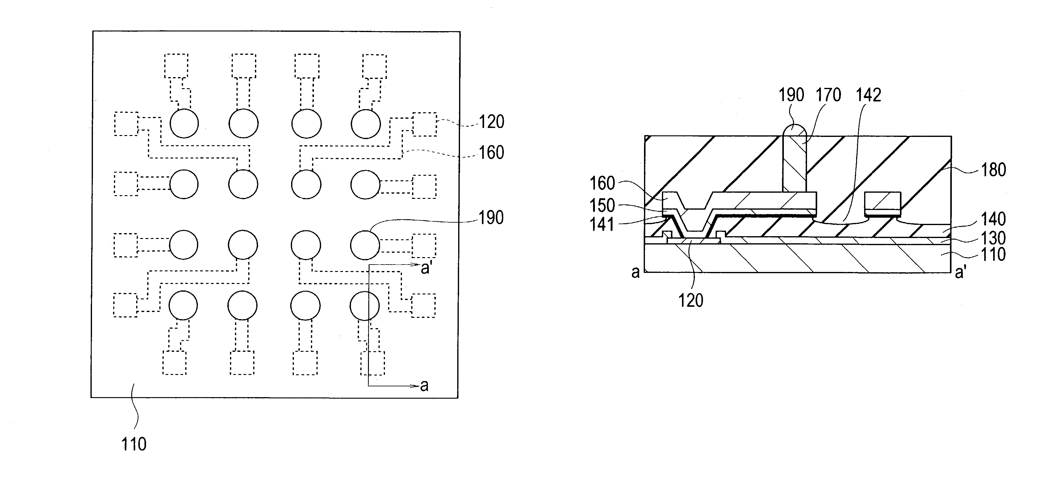
[0028]FIG. 1 shows a plan view of the structure of the essential parts of the semiconductor device according to this embodiment, FIG. 2 is a diagram of a section along the line a-a′ in FIG. 1.
[0029]As shown in FIGS. 1 and 2, the semiconductor device according to this embodiment comprises the substrate 110, electrode pad 120, protective film 130, interlayer film 140, metallic thin film 150, metallic wiring 160, bump 170, sealing film 180 and external terminal 190. Only the substrate 110, electrode pad 120, metallic wiring 160, and external terminal 190 are shown in FIG. 1.
[0030]The substrate 110 is, for example, rectangular in shape. The size of this substrate 110 is, for example, 8 mm×8 mm or 9 mm×9 mm. As mentioned below, this substrate 110 can be obtained by dicing the wafer after the sealing film 180 has been formed.
[0031]Integrated circuits (not shown in the figures) are formed on...
second embodiment
[0070]Next, a second embodiment of the present invention will be explained with reference to FIGS. 7 and 8.
[0071]FIG. 7 is a sectional diagram of this embodiment, corresponding to the cross section along line a-a′ in FIG. 1. In FIG. 7, wherever the same symbols are used as in FIG. 2, they refer to the same structural elements as in FIG. 2.
[0072]In the semiconductor according to this embodiment, the trench formed in the interlayer film 140 differs from that according to the first embodiment.
[0073]In this embodiment, the trench 701 is formed by means of plasmaetching. By using a plasmaetching method, it is possible to carry out highly anisotropic etching. In other words, when plasmaetching is used, even though the depth of the trench 701 is made large, the amount of etching in the direction parallel to the substrate 110 does not become very large. Therefore, the plasma etching can form a deep trench 701 without removing the interlayer film 140 directly below the metallic thin film ...
third embodiment
[0084]Next, the third embodiment of the present invention will be explained with reference to FIGS. 9, 10 and 11.
[0085]FIG. 9 is a sectional diagram of this embodiment, corresponding to the sectional view along line a-a′ in FIG. 1. In FIG. 9, wherever the same symbols are used as in FIG. 2, they refer to the same structural elements as in FIG. 2.
[0086]In this embodiment, the formation of the trench after the formation of the bump 170 as in each of the embodiments above does not take place and the trench 901 is formed at the same time as the etching of the interlayer film 140 for the purpose of exposing the center part of the electrode pad 120. In this embodiment, the surface of the interlayer film 140 is modified after the trench 901 is formed so that the modifying layer 902 is also formed on the surface of the trench 901.
[0087]The method of manufacturing this embodiment will be explained below in detail with reference to FIGS. 10 and 11.
[0088]Firstly, in the same way as in the firs...
PUM
Abstract
A semiconductor device and method has trenches for raising reliability. An electrode pad, with a protective film and an interlayer film which form an opening on top, are on a substrate. A rewiring pattern in contact with the electrode pad at this opening is on top of the interlayer film. A trench is etched outside the rewiring pattern. A bump is formed on top of the rewiring pattern. The rewiring pattern and the trench are covered by a sealing film that that exposes the upper end of the bump. An external terminal is formed on top of the bump. The trenches increase contact area and adhesion between the covering film and the sealing film. The rougher the surface of the trench the better the adhesion, which makes the sealing film stick better and the semiconductor device more reliable.
Description
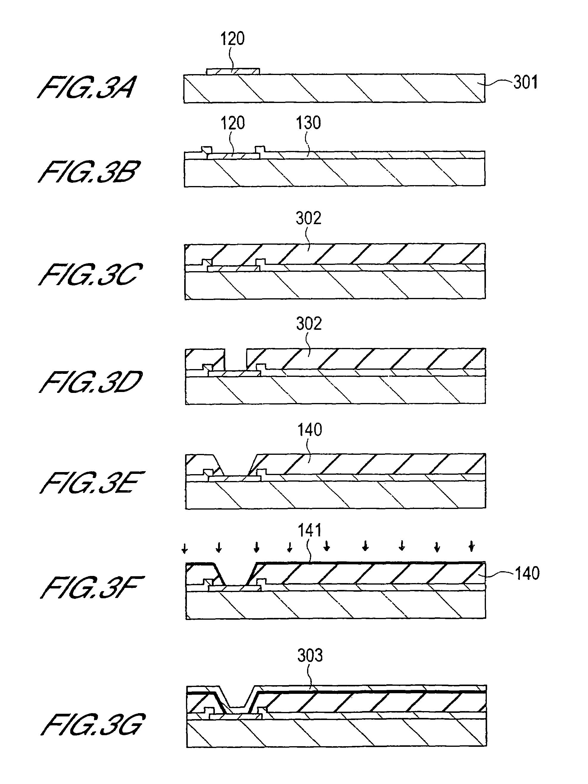
BACKGROUND OF THE INVENTION[0001]1. Field of the Invention[0002]The present invention relates to a semiconductor device in which a sealing film is formed on the surface of a substrate and a method for manufacturing said device. The present invention is applied, for example, to a semiconductor device which uses the wafer level chip size package method and to a method for manufacturing said device.[0003]2. Description of Related Art[0004]Wafer level chip size package (WCSP) technique is well known as a semiconductor manufacturing technique. WCSP is a technique in which resin sealing is performed before a dicing process.[0005]In WCSP a large number of integrated circuits is formed on the surface of a wafer, and then insulating films comprising protective films, interlayer films and the like are formed on the surface of the wafer so as to expose the center part of each of the electrode pads of these integrated circuits. Next, rewiring (redistribution wiring) patterns are formed on the s...
Claims
Application Information
Patent Timeline
Application Date:The date an application was filed.
Publication Date:The date a patent or application was officially published.
First Publication Date:The earliest publication date of a patent with the same application number.
Issue Date:Publication date of the patent grant document.
PCT Entry Date:The Entry date of PCT National Phase.
Estimated Expiry Date:The statutory expiry date of a patent right according to the Patent Law, and it is the longest term of protection that the patent right can achieve without the termination of the patent right due to other reasons(Term extension factor has been taken into account ).
Invalid Date:Actual expiry date is based on effective date or publication date of legal transaction data of invalid patent.

