Shielded through-via

a through-via and shielding technology, applied in the field of 3d interconnects, can solve the problems of increasing power consumption and heat dissipation, and achieve the effect of reducing the parasitic capacitance effect and high isolation from neighboring signals

Inactive Publication Date: 2009-09-15
TELEDYNE SCI & IMAGING
View PDF17 Cites 54 Cited by
  • Summary
  • Abstract
  • Description
  • Claims
  • Application Information

AI Technical Summary

Benefits of technology

[0011]The present invention provides a shielded through-via that reduces the effect of parasitic capacitance between the through-via and surrounding layer while providing high isolation from neighboring signals. The layer can be a wafer, a dielectric thin film in the multi-layer metal interconnect, a PCB layer, or a PCB layer in a multi-layer PCB structure.
[0012]A shield electrode is formed in an insulating region of the layer and spaced apart from the through-via. A coupling element couples at least a time-varying portion of the signal carried on the through-via to the shield electrode. This reduces the effect of any parasitic capacitance between the through-via and the shield electrode, hence the surrounding layer. In conductive or semi-conductive wafers, the shield electrode is also spaced apart from the wafer material. In resistive wafers or insulating layers such as PCBs or a thin-film dielectric, the through-via and shield electrode may be formed directly in the resistive or insulating material.

Problems solved by technology

One major challenge of 3D interconnects on a single wafer or in a wafer-to-wafer vertical stack is the through-via that provides a signal path for high impedance signals to traverse from one side of the wafer to the other.
Furthermore, loading increases power consumption and heat dissipation.

Method used


Image

  • Shielded through-via
  • Shielded through-via
  • Shielded through-via

Examples


Embodiment Construction

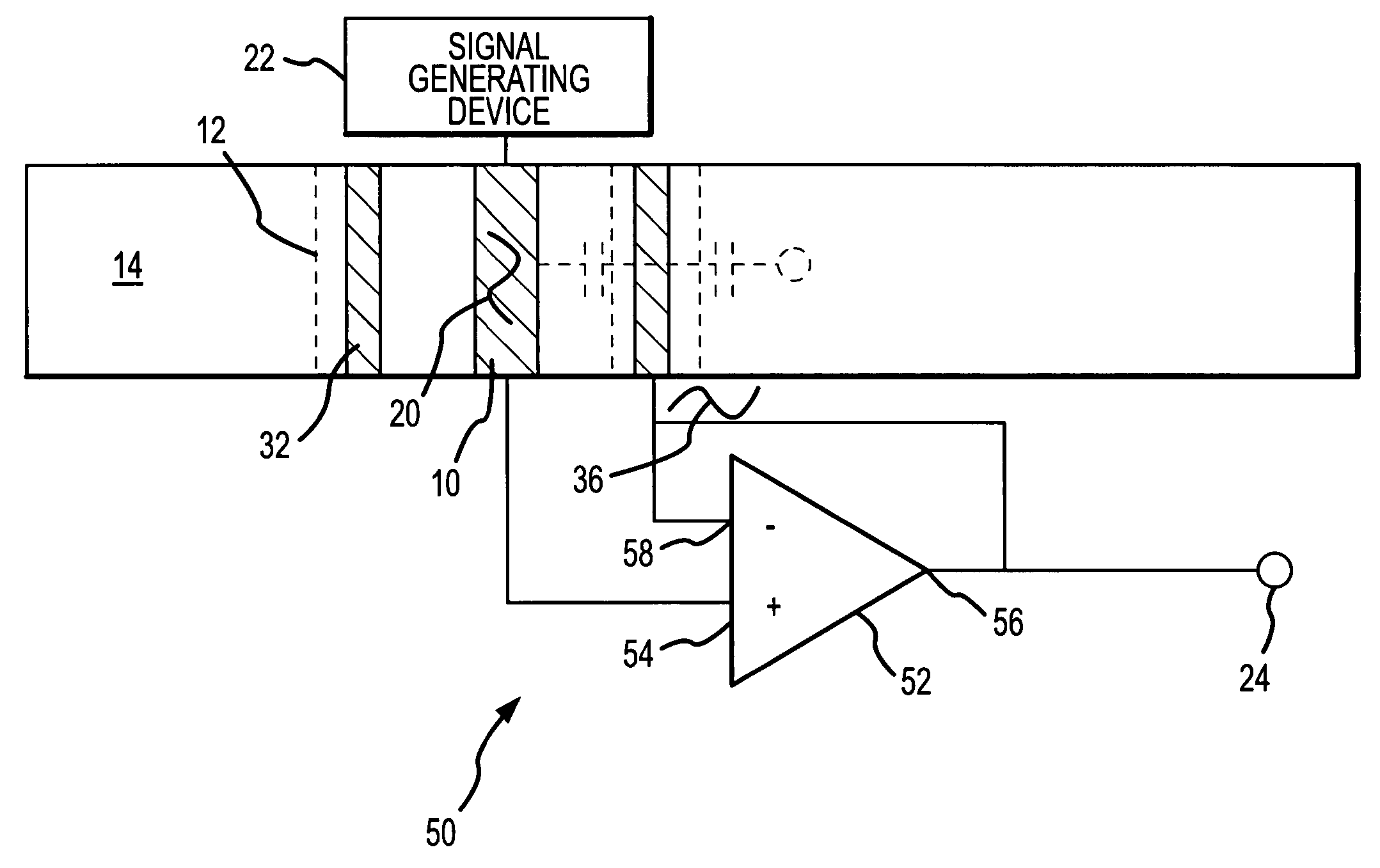
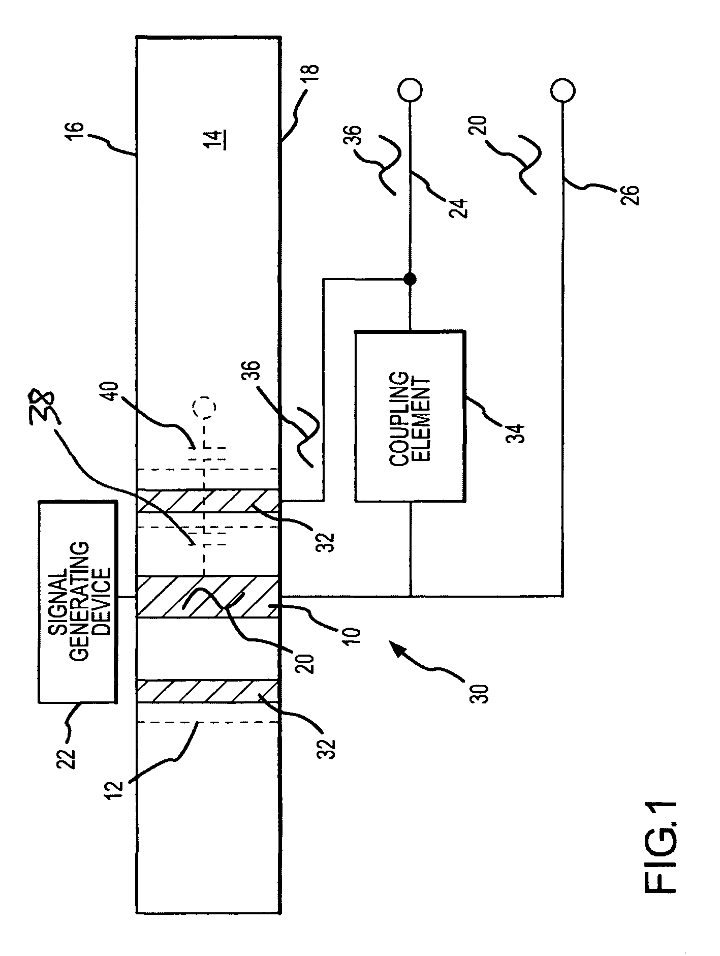
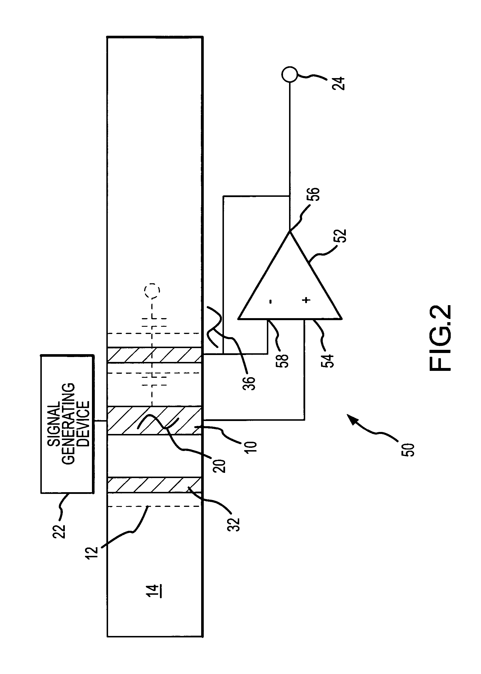
[0022]The present invention provides a shielded through-via that reduces the effect of parasitic capacitance between the through-via and surrounding layer while providing high isolation from neighboring signals. For purposes of illustration the shielded through-via will be described in the context of a semi-conductive wafer but it is understood that the layer can be, for example a wafer (conductive, semi-conductive or resistive), a dielectric thin film in a multi-layer metal interconnect on the surface of a wafer, a PCB layer, or a PCB layer in a multi-layer PCB structure.

[0023]As shown in FIG. 1, a through-via 10 is formed in an insulating region 12 of a wafer 14 and extends from a front surface 16 to a back surface 18. The through-via carries a signal 20 from a signal generating device 22 from the front surface to the back surface and to a conductive line 24 or 26. Typically, the signal will not include a DC component.

[0024]Absent the invention, the time-varying portion of the sig...


PUM


Abstract

A shielded through-via that reduces the effect of parasitic capacitance between the through-via and surrounding wafer while providing high isolation from neighboring signals. A shield electrode is formed in the insulating region and spaced apart from the through-via. A coupling element couples at least the time-varying portion of the signal carried on the through-via to the shield electrode. This reduces the effect of any parasitic capacitance between the through-via and the shield electrode, hence the surrounding wafer.

Description

BACKGROUND OF THE INVENTION[0001]1. Field of the Invention[0002]This invention relates to 3D interconnects for wafers, printed circuit boards (PCBs) and other high density circuits and more specifically to a shielded through-via that reduces the effect of parasitic capacitance on a high impedance signal passing through the through-via.[0003]2. Description of the Related Art[0004]Via connectors are widely used in the electronic industry for making electrical connections between the opposite surfaces of electronic devices. For example, in the manufacture of printed circuit board assemblies it is common practice to place discrete electronic components on one surface of a printed circuit board and to form the required connecting circuitry, ground planes, or the like on the opposite surface with the required electrical connections being made through the printed circuit board by using plated through holes or by various other techniques well known to those skilled in the printed circuit bo...

Claims


Application Information

Patent Timeline
Patent Type & Authority Patents(United States)
IPC IPC(8): H01L23/48
CPCH01L23/481H05K1/0222H05K1/0239H01L23/552H01L2924/0002H01L2223/6622H01L2225/06513H01L2225/06541H01L2924/3011H05K1/115H05K3/4602H05K2201/0959H05K2201/09645H05K2201/09809H01L2924/00H01L23/48
Inventor YAO, JUN JASON
Owner TELEDYNE SCI & IMAGING
Why Eureka
Try Eureka