Signal transmission structure and circuit substrate thereof

a signal transmission and circuit substrate technology, applied in the direction of printed circuit aspects, cross-talk/noise/interference reduction, electrical apparatus construction details, etc., can solve the problems of reducing the quality of transmitting signals, aggravate the impedance mismatch of signal transmission paths, etc., and achieve the effect of improving the signal transmission quality

Active Publication Date: 2007-11-06
VIA TECH INC
View PDF1 Cites 8 Cited by
  • Summary
  • Abstract
  • Description
  • Claims
  • Application Information

AI Technical Summary

Benefits of technology

[0011]Accordingly, one object of the present invention is directed to a signal transmission structure providing better impedance match to improve the signal transmission quality.
[0012]Another object of the present invention is directed to a signal transmission structure capable of reducing the parasitic capacitance effect of the reference planes and of improving the impedance mismatch while the signals pass through the two via landing pads.
[0015]In respect to the via landing pads and adjacent reference planes according to the present invention, each position of via landing pads is totally contained by the projected area of the opening formed by etching the reference planes. In other words, the areas where the non-perfect reference planes are projected on the planes of the via landing pads do not overlap with the via landing pads. Thus, when the signal passes through the non-prefect reference planes, the impedance can be more consistent. Accordingly, the present invention is capable of reducing the signal reflection due to the impedance mismatch of signal-transmitting path in the signal transmission and enhancing the signal transmission quality.

Problems solved by technology

It also means that it aggravates the impedance mismatch of the signal transmission path.
Furthermore it reduces the quality of the transmitting signals.

Method used


Image

  • Signal transmission structure and circuit substrate thereof
  • Signal transmission structure and circuit substrate thereof
  • Signal transmission structure and circuit substrate thereof

Examples


Embodiment Construction

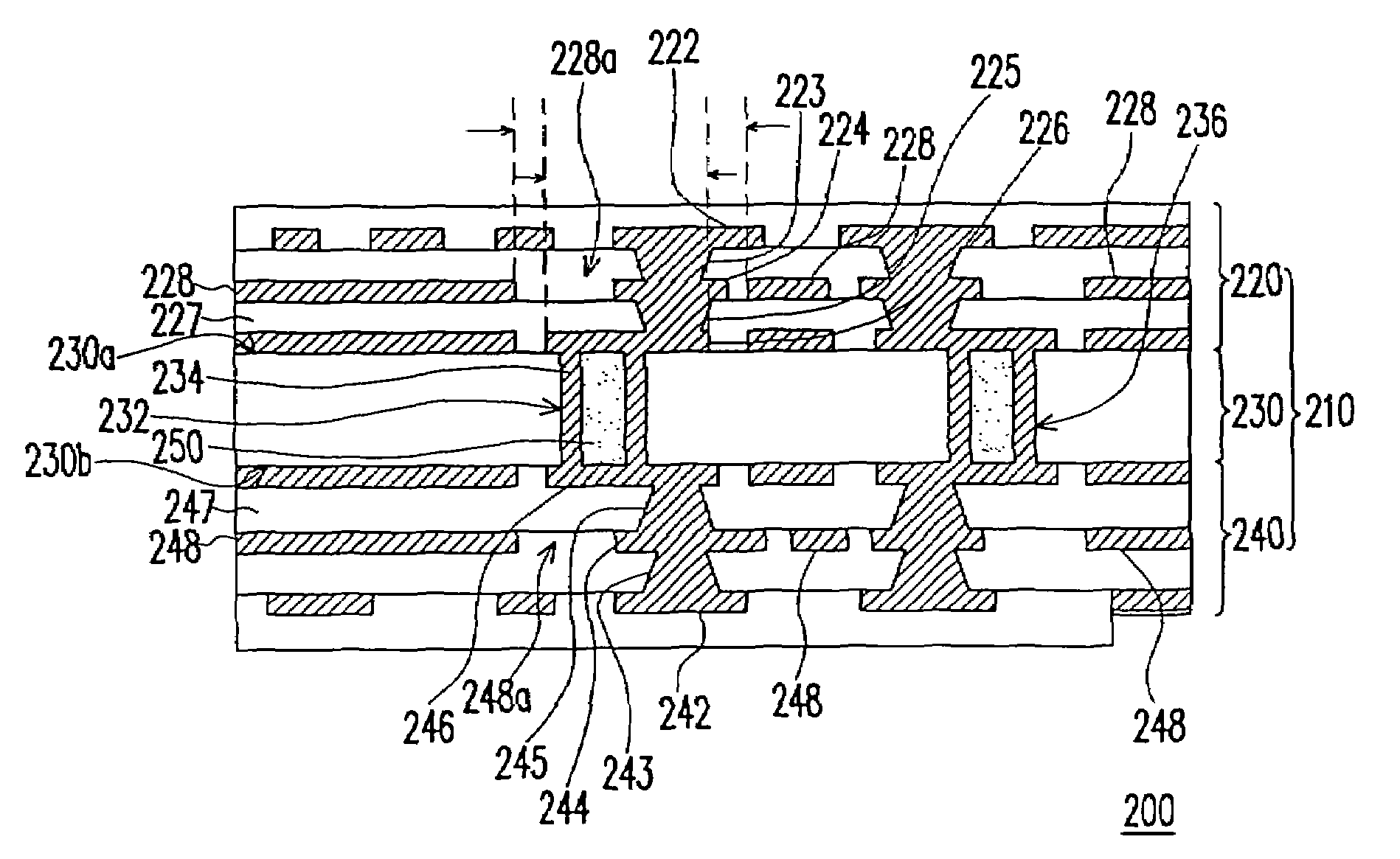
[0020]FIG. 2 schematically shows a cross-sectional view of a circuit substrate according to one embodiment of the present invention. Take a substrate having six patterned-circuit layers for example. The circuit substrate 200 has a stack layer 210 sequentially comprising a first circuit structure 220, a core layer 230, and a second circuit structure 240. Wherein, the two via landing pads 224, 226 of the first circuit structure 220 are electrically connected by a conducting via 225. A reference plane 228 is disposed on a first dielectric layer 227 above the via landing pad 226, serving as the reference of the electric potential for signal transmission in the first circuit structure. Besides, the two via landing pads 244, 246 of the second circuit structure 240 are electrically connected by a conducting via 245. A reference plane 248 is disposed on a second dielectric layer 247 above a via landing pad 246, serving as the reference of electric potential for signal transmission in the se...


PUM


Abstract

A signal transmission structure suitable for a multi-layer circuit substrate comprising a core layer and at least a dielectric layer is provided. The signal transmission structure according to the present invention comprises a first via landing pad and a reference plane. The first via landing pad is disposed on a first surface of the core layer, and covering one end of the through hole of the core layer. The dielectric layer covers the first via landing pad and the first surface of the core layer. And the first reference plane is disposed above the dielectric layer, having a first opening disposed above one end of the through hole. Wherein, the area where the first reference plane is projected on the first surface of the core layer does not overlap with the area where the first via landing pad is projected on the first surface of the core layer.

Description

CROSS-REFERENCE TO RELATED APPLICATION[0001]This application claims the priority benefit of Taiwan application serial no. 93129545, filed on Sep. 30, 2004. All disclosure of the Taiwan application is incorporated herein by reference.BACKGROUND OF THE INVENTION[0002]1. Field of Invention[0003]The present invention relates to a signal transmission structure. More particularly, the present invention relates a signal transmission structure and a circuit substrate thereof capable of reducing the impedance mismatch of the signal transmission path.[0004]2. Description of Related Art[0005]The common circuit substrates are composed of alternately stacked multiple patterned-circuit layers and multiple dielectric layers. For example, the patterned-circuit layers are formed on the copper foils through the photolithography process and etching process, and a part of the non-etched copper foils can serve as a reference plane of the circuit substrates, such as a ground plane or a power plane for ex...

Claims


Application Information

Patent Timeline
Patent Type & Authority Patents(United States)
IPC IPC(8): H01L23/48
CPCH05K1/0216H05K3/4602H05K2201/09718H05K2201/093H05K2201/0959H05K2201/0347
Inventor HSU, CHI-HSINGHSU, HSING-CHOU
Owner VIA TECH INC
Why Eureka
Try Eureka