Printed circuit board with improved hole

A technology of printed circuit boards and vias, which is applied in the fields of printed circuit, printed circuit, printed circuit manufacturing, etc. It can solve the problems of reducing circuit speed, prolonging signal rise time, distortion, etc., and achieves the goal of improving characteristic impedance and signal transmission quality Effect

Inactive Publication Date: 2007-02-14
HONG FU JIN PRECISION IND (SHENZHEN) CO LTD +1
View PDF0 Cites 21 Cited by
  • Summary
  • Abstract
  • Description
  • Claims
  • Application Information

AI Technical Summary

Problems solved by technology

The first pad 310 and the second pad 330 of the buried hole 34 will couple with the adjacent plane layer to generate parasitic capacitance. The impact of the parasitic capacitance on the circuit is to prolong the rise time of the signal and reduce the speed of the circuit. Distorted when transmitted

Method used


Image

  • Printed circuit board with improved hole
  • Printed circuit board with improved hole
  • Printed circuit board with improved hole

Examples


Embodiment Construction

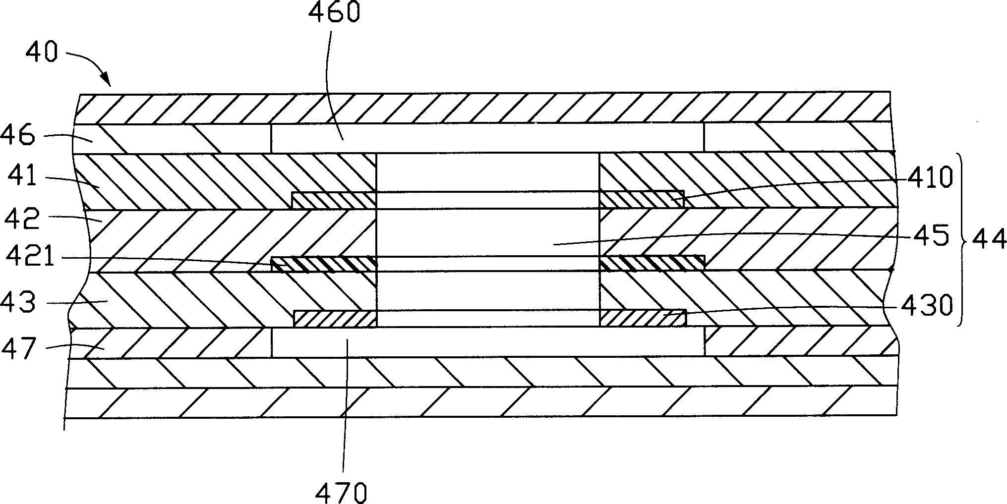
[0015] Please refer to figure 2 , which is a cross-sectional view of a printed circuit board with improved vias in the first preferred embodiment of the present invention, the printed circuit board 40 is an eight-layer board, which includes a first plane layer 41 and a second plane layer 43 , a third planar layer 47, a fourth planar layer 42, a fifth planar layer 46 and a buried hole 44, the buried hole 44 includes a drilled hole 45, a first pad 410 and a second pad 430, the diameter of the first pad 410 is the same as that of the second pad 430, the first pad 410 is located on the first planar layer 41, and the second pad 430 is located on the On the second plane layer 43, the first plane layer 41 and the second plane layer 43 are signal layers, and the first pad 410 and the second pad 430 are used for the drilling 45 and the first plane layer. The connection of traces on the layer 41 and the second plane layer 43 . The drill hole 45 runs through the first plane layer 41, ...


PUM


Abstract

The invention relates to a kind of printed circuit board with improved holes, including a first planar layer, a second planar layer, a third planar layer and a hole. The described hole includes a bored hole, a first bond pad and a second bond pad. The described first bond pad is located above the first planar layer. The described second bond pad is located above the second planar layer. The described bored hole is drilled through the first planar layer and the second planar layer. The described third planar layer is hollowed to form of a hole at the corresponding part of the second bond pad. This invention can improve the characteristic impedance to improve signal transmission quality.

Description

【Technical field】 [0001] The invention relates to a printed circuit board (Printed Circuit Board), in particular to a printed circuit board with improved via holes to improve signal integrity. 【Background technique】 [0002] With the improvement of the output switching speed of integrated circuits and the increase of the wiring density of printed circuit boards, signal integrity has become one of the issues that must be concerned in the design of high-speed digital printed circuit boards. Factors such as the parameters of components and printed circuit boards, the layout of components on printed circuit boards, and the routing of high-speed signals can all cause signal integrity problems. [0003] At present, due to the increase of signal density on the printed circuit board, the number of signal transmission layers also increases accordingly, so it is inevitable to realize inter-layer signal transmission through via holes. Vias are one of the important components of multil...

Claims


Application Information

Patent Timeline
Patent Type & Authority Applications(China)
IPC IPC(8): H05K1/11H05K1/16
CPCH05K3/429H05K1/024H05K2201/09536H05K1/0272H05K1/115
Inventor 林有旭叶尚苍黄肇振李传兵
Owner HONG FU JIN PRECISION IND (SHENZHEN) CO LTD
Why Eureka
Try Eureka