Signal transmission structure and layout method for the same

a signal transmission and layout method technology, applied in the direction of printed circuit details, cross-talk/noise/interference reduction, printed circuits, etc., can solve the problems of increasing production costs, increasing production costs, and complex power plane metal layer structure, etc., to reduce the equivalent capacitance, increase the characteristic impedance of the neck block, and reduce the effect of electromagnetic transmission between adjacent conduction blocks

Inactive Publication Date: 2009-03-05
TATUNG COMPANY
View PDF6 Cites 6 Cited by
  • Summary
  • Abstract
  • Description
  • Claims
  • Application Information

AI Technical Summary

Benefits of technology

[0009]Accordingly, the present invention is directed to a signal transmission structure. The signal transmission structure includes conduction blocks periodically formed at a power plane, neck blocks connecting adjacent conduction blocks, and openings formed corresponding to the neck blocks at a ground plane for reducing equivalent capacitance between the neck blocks and the ground plane. The signal transmission structure improves the performance of isolating electromagnetic noise by increasing a characteristic impedance of the neck blocks.
[0010]The present invention is also directed to a layout method for a signal transmission structure. The layout method includes providing a patterned layout to obtain the aforementioned signal transmission structure for improving the noise filtering performance of the power plane and suppressing the noise propagation capability.
[0018]The present invention correspondingly disposes openings at the ground plane to reduce the equivalent capacitance between the ground plane and the power plane to further increase the characteristic impedance of the neck block. In such a way, the electromagnetic transmission between adjacent conduction blocks is lowered, and the noise isolation performance can be improved accordingly. Further, the neck blocks need not be thin and long, and therefore the layout of the power plane can be simplified to improve signal quality. Meanwhile, the corresponding opening need not be too large so that the metal layer of the ground plane is substantially complete. As such, the signal transmission structure according to the present invention is adapted to improve the signal quality and noise isolation performance when working at a high frequency.

Problems solved by technology

However, this structure still has a disadvantage in that three metal layers are required, and the vias 121 are further required to configure in the PCB for connecting the embedded metal blocks 111 and the bottom metal layer, i.e., the ground plane 120, both of which increase production costs thereof.
However, the performance of the single layer metal cutting structure shown in FIG. 2 is not as good as that of structure shown in FIG. 1.
Unfortunately, this makes the power plane metal layer too complicated so as to cause discontinuity in return current path of adjacent signal line layer.

Method used


Image

  • Signal transmission structure and layout method for the same
  • Signal transmission structure and layout method for the same
  • Signal transmission structure and layout method for the same

Examples


first embodiment

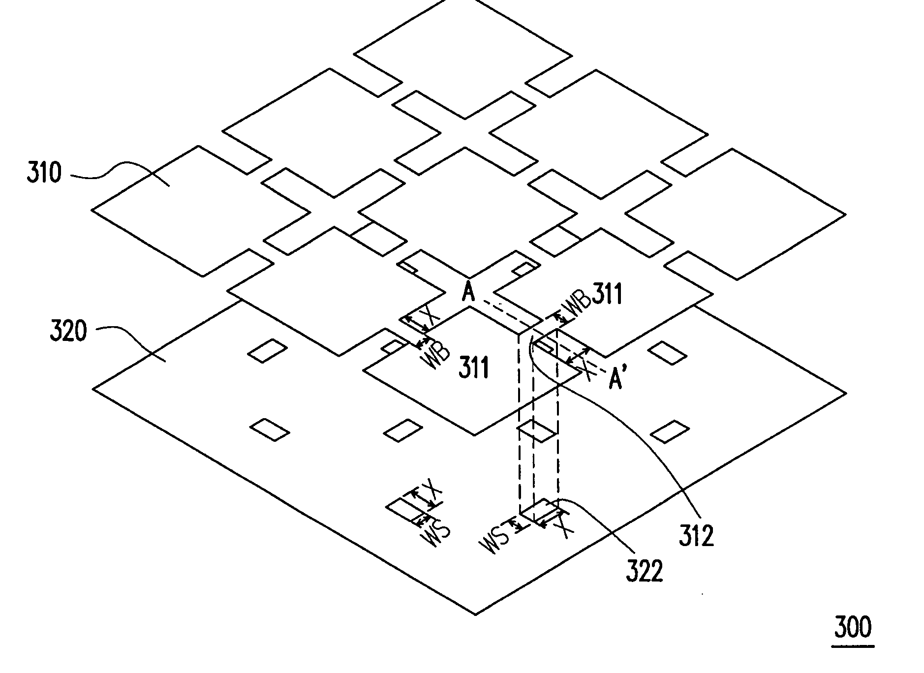
[0034]FIG. 3 is a schematic diagram illustrating a signal transmission structure according to a first embodiment of the present invention. Referring to FIG. 3, there is shown a signal transmission structure 300. The signal transmission structure 300 includes a first reference plane 310 and a second reference plane 320. According to an aspect of the first embodiment, the first reference plane 310, for example, is a power plane, and the second reference plane 320, for example, is a ground plane.

[0035]The first reference plane 310 is composed of a plurality of conduction blocks 311. A connecting channel connecting adjacent conduction blocks 311 is defined as a neck block 312. The first reference plane 310 is composed of periodically formed conduction blocks 311 and neck blocks 312. The second reference plane 320 and the first reference plane 310 are adjacent one to another, such as adjacent upper and bottom surfaces or different metal layers of a PCB. The second reference plane 320 has...

second embodiment

[0045]FIG. 6 is a schematic diagram illustrating a signal transmission structure according to a second embodiment of the present invention. Referring to FIG. 6, a signal transmission structure 600 includes a first reference plane 610, and a second reference plane 620. The first reference plane 610 for example is a power plane, and the second reference plane 620 for example is a ground plane.

[0046]The first reference plane 610 is composed of a plurality of orthohexagonal conduction blocks 611 which are periodically formed. Adjacent conduction blocks 611 are connected by neck blocks 612. The second reference plane 620 includes a plurality of openings 622 formed at positions corresponding to the neck blocks 612 for decreasing an equivalent capacitance between the neck blocks 612 and the second reference plane 620. Now referring to FIGS. 7A and 7B, there are shown structural diagrams of respectively the first reference plane and the second reference plane and layouts thereof according t...

third embodiment

[0050]According to another aspect, the present invention provides a layout method for a signal transmission structure. As shown in FIG. 9, there is shown a flow chart of a layout method according to the third embodiment of the present invention. The layout method includes: periodically forming a plurality of conduction blocks at a first reference plane (step S910); forming at least one neck block to connect adjacent conduction blocks, wherein when there are only two conduction blocks formed at the first reference plane, and only one neck block needed for connecting the two conduction blocks (step S920); and forming at least one opening at a second reference plane at a position corresponding to the neck block, in which the first reference plane and the second reference plane are adjacent one to another (step S930).

[0051]In the step S930, the opening can be larger than, smaller than or equivalent to the neck block. The present invention can be applied to a PCB, in which the first refe...


PUM


Abstract

A signal transmission structure is provided. The signal transmission structure includes conduction blocks periodically formed at a power plane, neck blocks connecting adjacent conduction blocks, and openings formed corresponding to the neck blocks at a ground plane for reducing equivalent capacitance between the neck blocks and the ground plane, so as to improve the noise isolation performance.

Description

CROSS-REFERENCE TO RELATED APPLICATION[0001]This application claims the priority benefit of Taiwan application serial no. 96133057, filed on Sep. 5, 2007. The entirety of the above-mentioned patent application is hereby incorporated by reference herein and made a part of this specification.BACKGROUND OF THE INVENTION[0002]1. Field of the Invention[0003]The present invention generally relates to a signal transmission structure, and more particularly, to a signal transmission structure of a power plane and a ground plane, and a layout method for the signal transmission structure.[0004]2. Description of Related Art[0005]In order to prevent propagation of electromagnetic noise in a printed circuit board (PCB), decoupling capacitors are often provided to filter the electromagnetic noise. However, because of the equivalent series inductance of the capacitors, the effective noise filtering bands for decoupling capacitors are usually below 500 MHz.[0006]In higher frequency bands, for exampl...

Claims


Application Information

Patent Timeline
Patent Type & Authority Applications(United States)
IPC IPC(8): H05K1/02
CPCH05K1/0236H05K2201/0969H05K2201/09681H05K2201/09309
Inventor CHAO, SHIH-CHIEHHUANG, CHIH-WENLIAO, CHUN-LIN
Owner TATUNG COMPANY
Why Eureka
Try Eureka