Wireless frequency power amplifier, semiconductor device, and wireless frequency power amplification method

Inactive Publication Date: 2008-09-25
PANASONIC CORP
View PDF9 Cites 19 Cited by
  • Summary
  • Abstract
  • Description
  • Claims
  • Application Information

AI Technical Summary

Benefits of technology

[0023]The present invention is directed to solving the foregoing problems of the prior art, and an object of the invention is to stabilize the operation of a wireless frequency power amplifier that amplifies m

Problems solved by technology

If shielded materials which consist of metal or other conductors come close to the antenna, the high frequency power amplifier is mismatched because of the impedance fluctuation of the antenna.
This fluctuation degrades the reliability of the high frequency power amplifier performance.
This fluctuation can also cause the undesirable oscillations of the final amplification stage transistor, resulting in transistor failure due to excessive heating.
The impedance fluctuation noted above affects the high linearity operation of the high frequency power amplifier and causes unstable operation of the high performance transistors in the high frequency power amplifier.
The unstable operation of the high performance transistors causes the distortion of the high frequency power amplifier, resulting in the degradation of the transmission performance of the cell phones and wireless devices.
However, isolators, circulators, and other such unilateral components include a magnet, ferrite, or other such material, imposing a significant limitation on the size and weight reduction and degree of integration that can be achieved.
However, because the isolator 93 includes ferrite or a permanent magnet, for example, the isolator 93 interferes not only with reducing the size but also reducing the weight of the cell phone or other mobile communication device.
This is a factor increasing the power consumption of the wireless frequency power amplifier, which either shortens the connection time of the cell phone or requires increa

Method used


Image

  • Wireless frequency power amplifier, semiconductor device, and wireless frequency power amplification method
  • Wireless frequency power amplifier, semiconductor device, and wireless frequency power amplification method
  • Wireless frequency power amplifier, semiconductor device, and wireless frequency power amplification method

Examples


embodiment 1

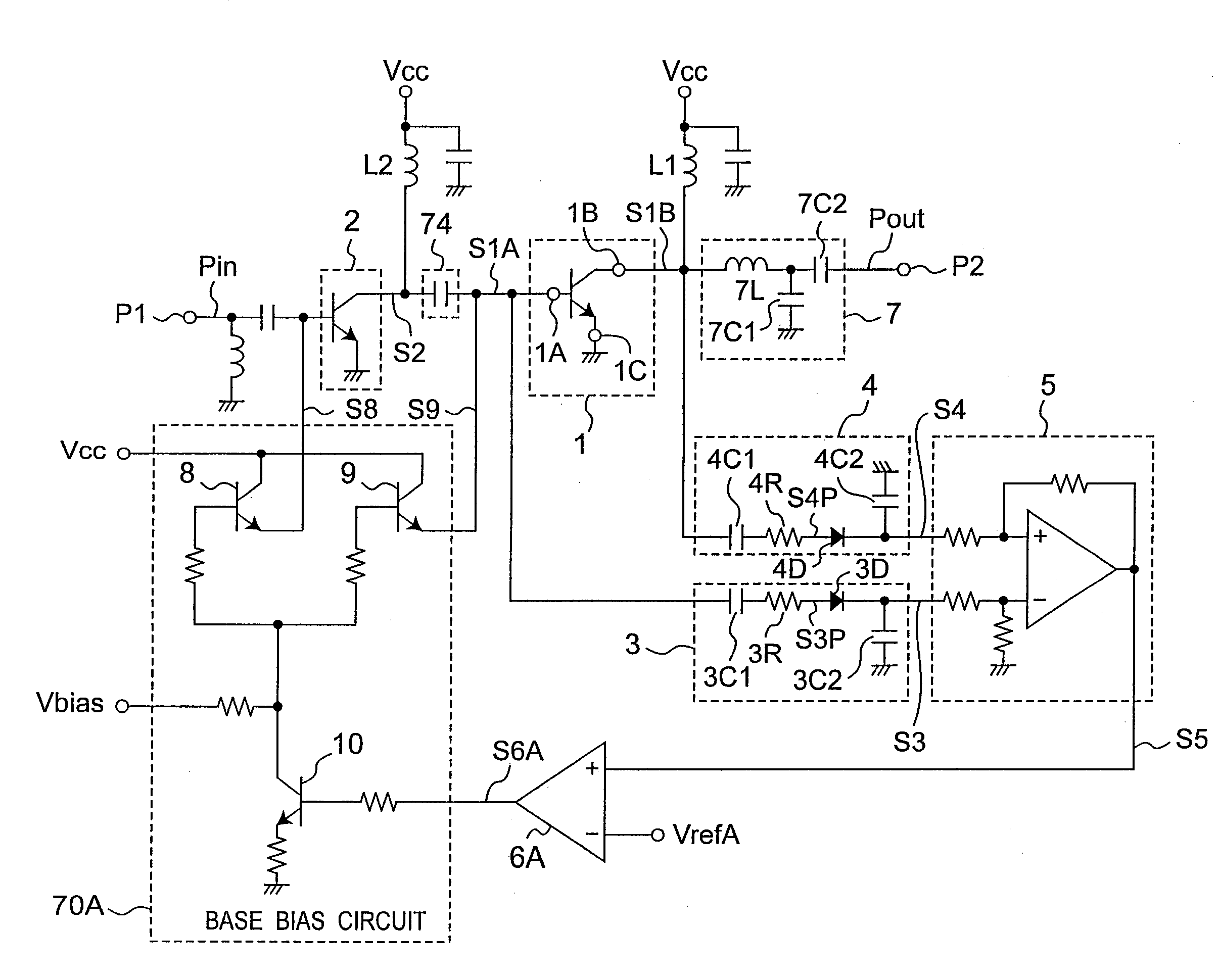
[0059]FIG. 1 is an equivalent circuit diagram showing an example of a wireless frequency power amplifier according to a first embodiment of the invention. As shown in FIG. 1 the wireless frequency power amplifier according to this first embodiment has a transistor 1, a matching circuit 7, and a drive stage 2. An amplifier input signal Terminal is input to the amplifier input node P1. The transistor 1 is also referred to as final stage 1 or amplification stage 1 below. The drive stage 2 is also referred to as amplification stage 2, and the amplifier input signal Terminal is also referred to as a modulation signal.[0060]The modulation signal is generated by modulating a carrier wave with a signal to be modulated based on the modulation method. In the case of a cell phone the signal to be modulated is a voice signal or an Internet data signal, and is an Internet data signal in the case of a wireless local area network (WLAN). In this case, the phase and amplitude of the modulation sign...

embodiment 2

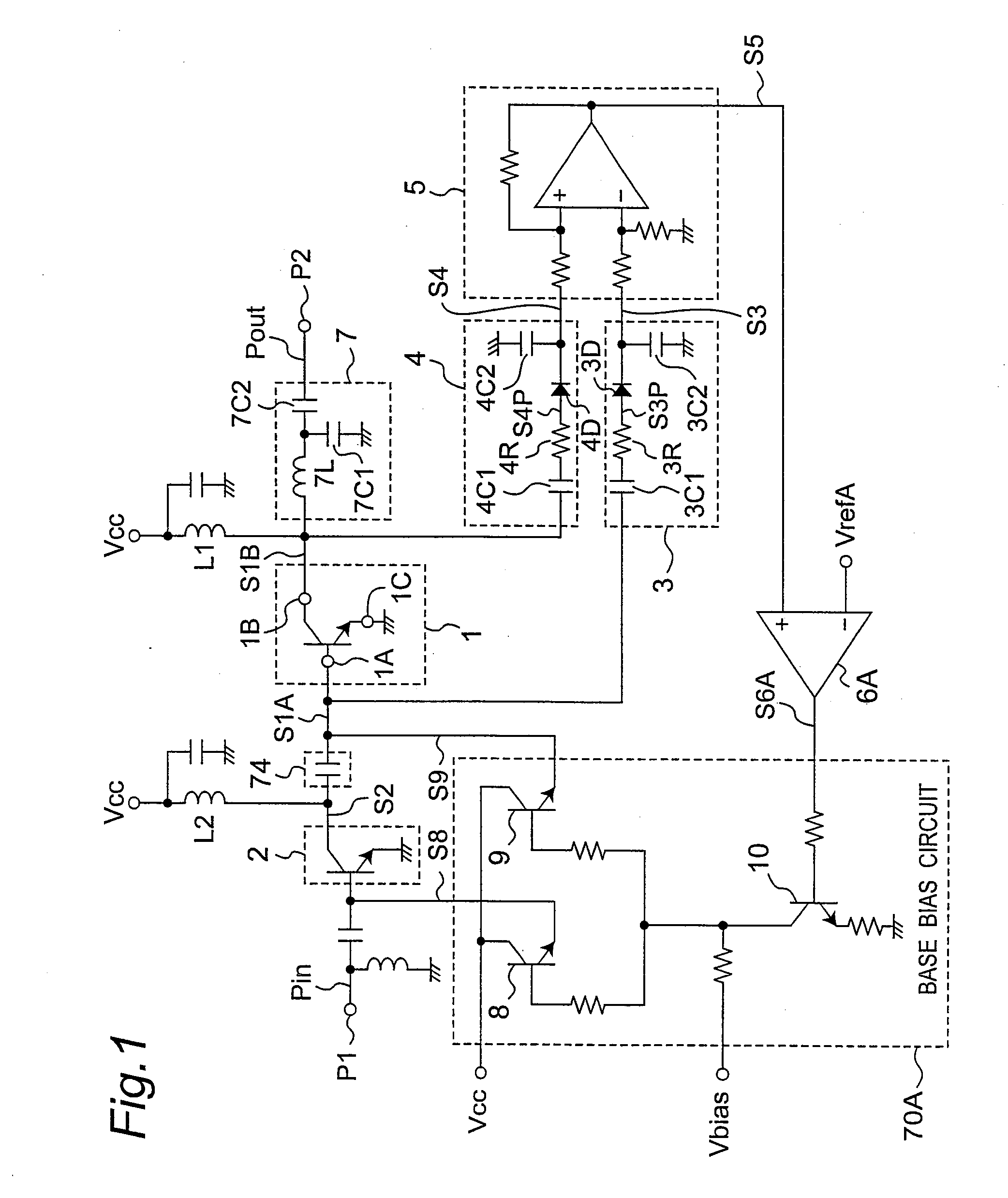
[0085]A wireless frequency power amplifier according to a second embodiment of the invention is described next. Primarily the differences between this embodiment and the first embodiment are described below. Other aspects of the arrangement, operation, and effect of this embodiment are the same as in the first embodiment, and further description thereof is therefore omitted.

[0086]FIG. 2 is an equivalent circuit diagram showing an example of a wireless frequency power amplifier according to a second embodiment of the invention. In the second embodiment as shown in FIG. 2, the base bias circuit 70B outputs predetermined base bias currents S8 and S9 based on a predetermined voltage Vbias without being controlled by the comparator output voltage S6A. In addition, the supply voltage Vcc1 is supplied from a battery 73 through a regulator circuit 72. The supply voltage Vcc1 contains the power supply current, and is therefore also referred to as dc power. The regulator circuit 72 is also re...

embodiment 3

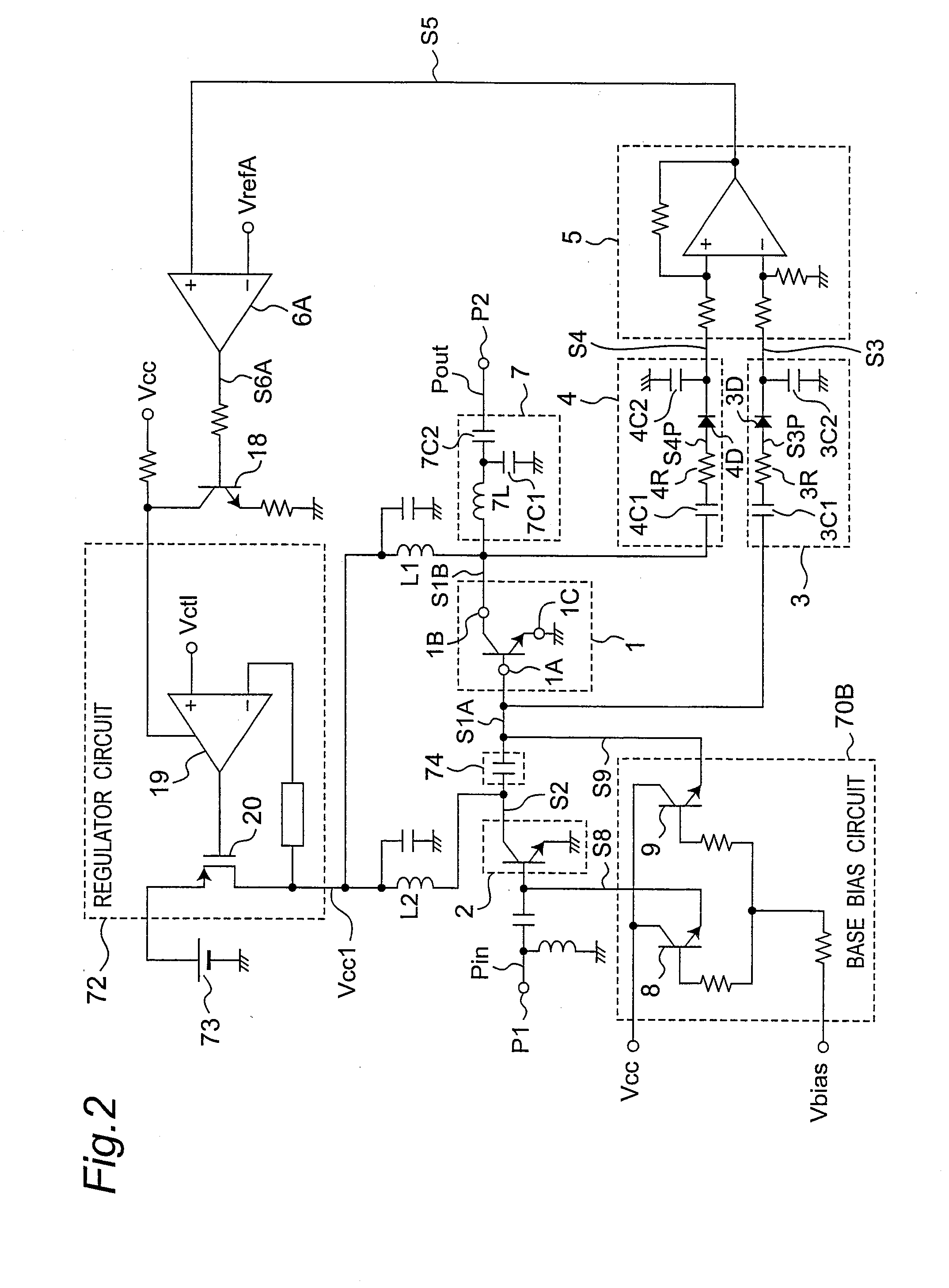
[0092]A wireless frequency power amplifier according to a third embodiment of the invention is described next. Primarily the differences between this embodiment and the first embodiment are described below. Other aspects of the arrangement, operation, and effect of this embodiment are the same as in the first embodiment, and further description thereof is therefore omitted.

[0093]FIG. 3 is an equivalent circuit diagram showing an example of a wireless frequency power amplifier according to a third embodiment of the invention. In the third embodiment as shown in FIG. 3, the base bias circuit 70B outputs predetermined base bias currents S8 and S9 based on a predetermined voltage Vbias without being controlled by the comparator output voltage S6A. In addition, the wireless frequency power amplifier also has a stabilization circuit 28 inserted between the input node 1A and the emitter node 1C (ground node) of the transistor 1. The arrangement including the stabilization circuit 28 and th...


PUM


Abstract

A differential amplifier circuit is connected to the input node and the output node of the final amplification stage through detection circuits. The signal level difference output from the differential amplifier circuit does not change even if the input power varies. Because a change in the power gain at the output node does not travel back to the input node when the load impedance of the wireless frequency power amplifier varies, it is possible to detect only the change in the load impedance. Damage to the final stage can be prevented by controlling the operating current of the final stage and the gain of the drive stage according to the detected load variation. Nonlinear distortion in the wireless frequency power amplifier output can also be reduced by detecting and canceling the change in the gain of the drive stage by changing the gain of the adjustment stage.

Description

BACKGROUND OF THE INVENTION[0001]1. Field of Invention[0002]The present invention relates to technology for amplifying wireless frequency signals in mobile wireless communication devices such as cell phones that are small, lightweight, and low current consumption, and more particularly relates to technology for a wireless frequency power amplifier, a semiconductor device, and a wireless frequency power amplification method.[0003]2. Description of Related Art[0004]Mobile wireless communication devices such as cell phones have a wireless frequency power amplifier which enables amplification of high frequency signals. Output signals of the high frequency power amplifier are transmitted to a base station through the antenna of the mobile wireless communication devices. The high frequency power amplifier is required to be small, inexpensive, and low current consumption. High performance transistors such as GaAs-FET (gallium arsenide field-effect transistors), HBT (heterojunction bipolar ...

Claims


Application Information

Patent Timeline
IPC IPC(8): H03F3/16H03G3/00
CPCH03F1/30H03G3/3042H03F3/19
Inventor SUZAKI, HIDEFUMIITO, JUNJIKAMIMURA, FUMIYANAKAMURA, SHIGEKI
Owner PANASONIC CORP
Why Eureka
Try Eureka