Stacked semiconductor device and printed circuit board

Active Publication Date: 2014-03-13
CANON KK
View PDF0 Cites 3 Cited by
  • Summary
  • Abstract
  • Description
  • Claims
  • Application Information

AI Technical Summary

Benefits of technology

The present invention aims to improve the quality of power supply to a second semiconductor element to stabilize its signal processing operation while ensuring the wiring capability of the motherboard. This results in a more stable and reliable power supply for the second semiconductor element, leading to improved performance and reliability of the overall system.

Problems solved by technology

However, the technology described in Japanese Patent Application Laid-Open No. 2009-182087 is not always sufficient for further decreasing the inductance.
In the case of a printed wiring board in which a via of the build-up layer is connected immediately above a via of the core layer, the yields are low and the cost is high.
In this configuration, however, it is difficult to take out a signal wiring of a surface layer of the mother board on which the stacked semiconductor device is mounted.

Method used


Image

  • Stacked semiconductor device and printed circuit board
  • Stacked semiconductor device and printed circuit board
  • Stacked semiconductor device and printed circuit board

Examples


first embodiment

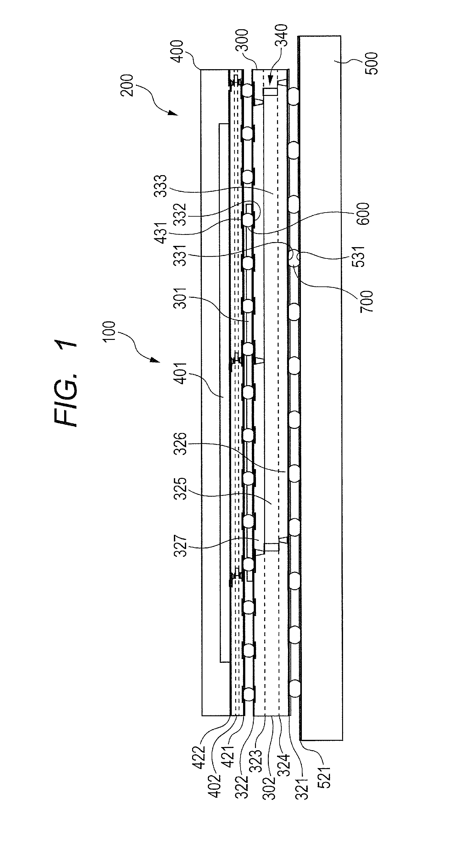
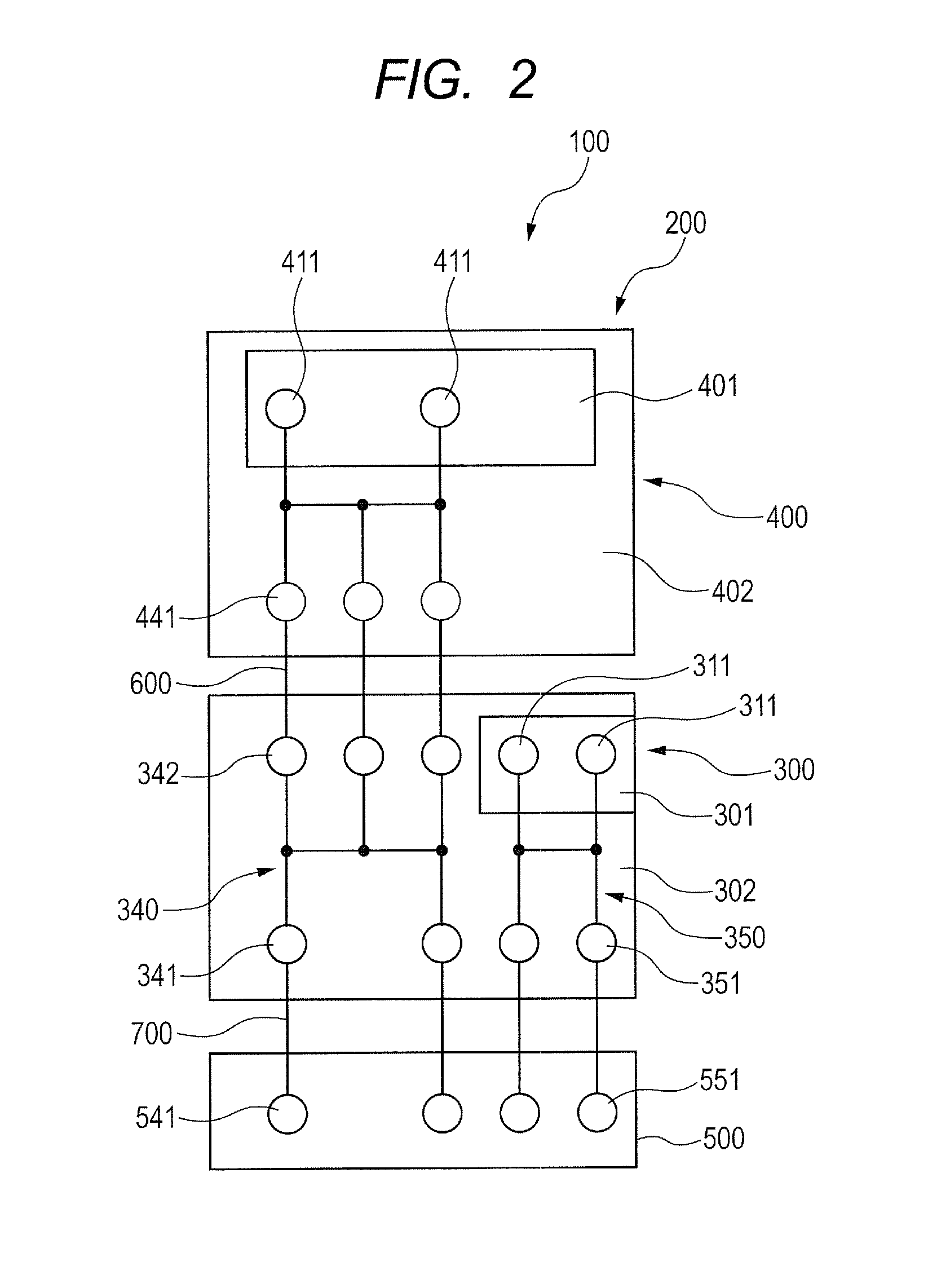
[0033]FIG. 1 is a cross-sectional view illustrating a schematic configuration of a printed circuit board including a stacked semiconductor device according to a first embodiment of the present invention. FIG. 2 is a schematic diagram of the printed circuit board including the stacked semiconductor device according to the first embodiment of the present invention.

[0034]A printed circuit board 100 includes a stacked semiconductor device 200, and a mother board 500 on which the stacked semiconductor device 200 is mounted. The stacked semiconductor device 200 is a stacked semiconductor package having a package-on-package (PoP) structure. The stacked semiconductor device 200 includes a lower semiconductor package 300 as a first semiconductor package and an upper semiconductor package 400 as a second semiconductor package, and the semiconductor package 400 is stacked on the semiconductor package 300.

[0035]The semiconductor package 300 includes a lower semiconductor element 301 as a first ...

second embodiment

[0062]Next, a description is given of a printed circuit board including a stacked semiconductor device according to a second embodiment of the present invention. FIG. 5 is a schematic diagram of the printed circuit board including the stacked semiconductor device according to the second embodiment of the present invention. FIGS. 6A to 6D are plan views illustrating respective layers of a first interposer. FIG. 6A illustrates a first layer, FIG. 6B illustrates a second layer, FIG. 6C illustrates a third layer, and FIG. 6D illustrates a fourth layer. Note that, in the second embodiment, similar components to those in the first embodiment are denoted by the same reference symbols to omit descriptions.

[0063]A printed circuit board 100A according to the second embodiment includes a stacked semiconductor device 200A, and a mother board 500A on which the stacked semiconductor device 200A is mounted. The stacked semiconductor device 200A is a stacked semiconductor package having a package-o...

third embodiment

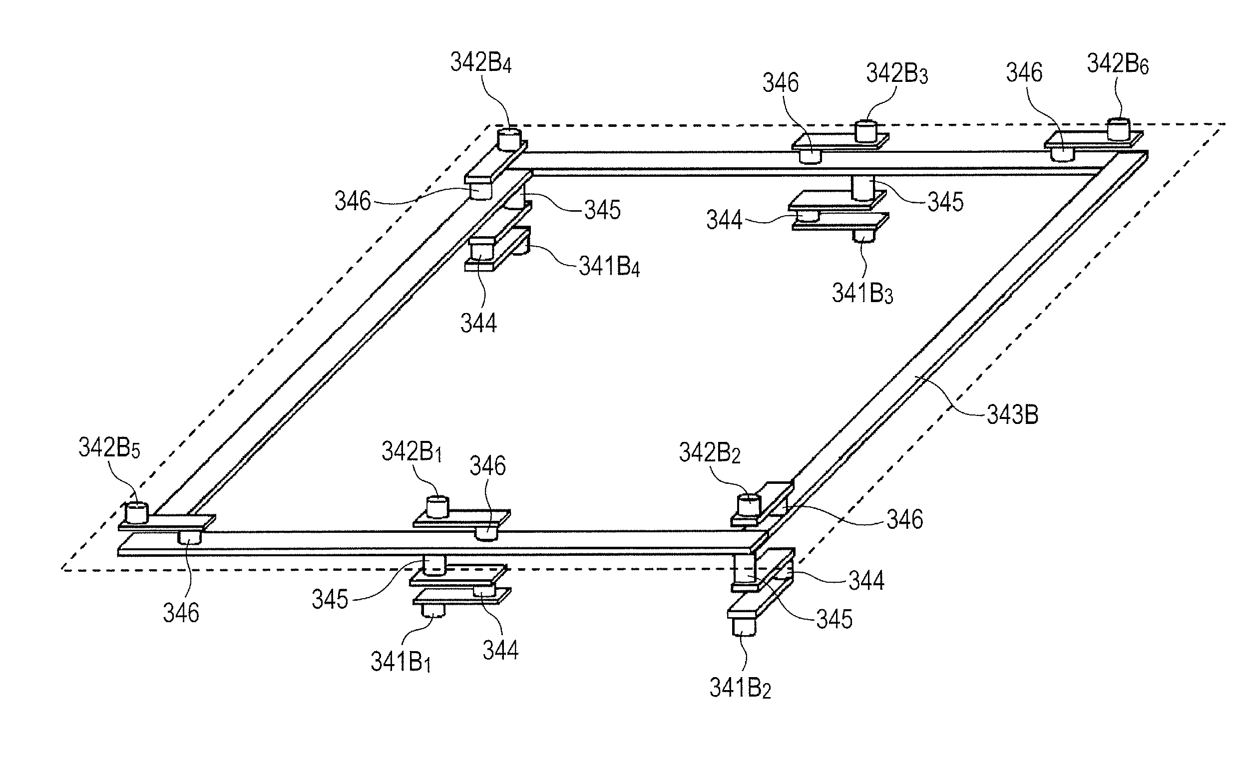
[0085]Next, a description is given of a printed circuit board including a stacked semiconductor device according to a third embodiment of the present invention. FIG. 10 is a schematic diagram of the printed circuit board including the stacked semiconductor device according to the third embodiment of the present invention. FIGS. 11A to 11D are plan views illustrating respective layers of a first interposer. FIG. 11A illustrates a first layer, FIG. 11B illustrates a second layer, FIG. 11C illustrates a third layer, and FIG. 11D illustrates a fourth layer. Note that, in the third embodiment, similar components to those in the first embodiment are denoted by the same reference symbols to omit descriptions.

[0086]A printed circuit board 100B according to the third embodiment includes a stacked semiconductor device 200B, and a mother board 500B on which the stacked semiconductor device 200B is mounted. The stacked semiconductor device 200B is a stacked semiconductor package having a packag...


PUM


Abstract

An interposer of a first semiconductor package includes a power supply wiring for a second semiconductor element, the power supply wiring including a land provided in one surface layer, and a power supply pattern provided in an inner layer and electrically connected to the land, the power supply wiring further including a larger number of lands than the land, which are provided in another surface layer and electrically connected in parallel to the power supply pattern. In a stacked semiconductor device, this configuration can improve the quality of power supply to the second semiconductor element to secure signal processing operation while preventing an increase in inductance caused by the bending of a power supply path in a power supply wiring of a printed wiring board or by a deviation of connection intervals.

Description

BACKGROUND OF THE INVENTION[0001]1. Field of the Invention[0002]The present invention relates to a stacked semiconductor device in which semiconductor packages are stacked, and a printed circuit board including the stacked semiconductor device.[0003]2. Description of the Related Art[0004]In recent years, along with the sophistication and miniaturization of electronic devices, demands have been growing for sophisticated and miniaturized electronic components and semiconductor devices used in the electronic devices. A semiconductor package called “ball grid array (BGA)” is known as the structure for realizing a high-pin count and compact semiconductor device. For further miniaturization, a stacked semiconductor device called “package-on-package (PoP)” is known, in which a semiconductor package including a memory semiconductor element is stacked on a semiconductor package including a logic semiconductor element, for example.[0005]The stacked semiconductor device is advantageous in that...

Claims


Application Information

Patent Timeline
IPC IPC(8): H01L23/00
CPCH01L24/25H01L2924/15311H01L23/50H01L25/105H01L2225/1023H01L2225/1058H01L2924/1434H01L2924/15331H01L2924/30107H01L23/49827H01L23/49833H01L23/49838
Inventor SUGIMOTO, SATOSHIKAWASE, YOSHITAKA
Owner CANON KK
Why Eureka
Try Eureka