

Liquid crystal display device
- Summary
- Abstract
- Description
- Claims
- Application Information
AI Technical Summary
Benefits of technology
Problems solved by technology
Method used
Image

Examples
first embodiment
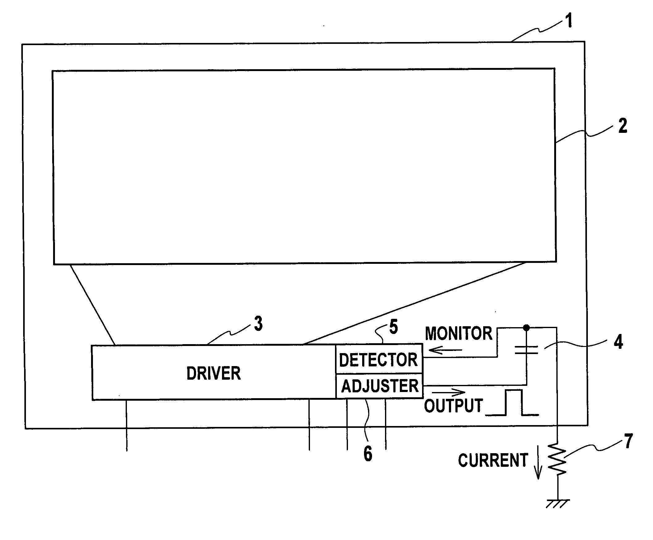
[0048] As shown in the schematic block diagram of FIG. 1, a liquid crystal display device of this embodiment includes an array substrate 1 in which a display section 2, a driver 3, and a detection capacitance 4 are formed on a translucent substrate. In order to enable transistors of each circuit to be formed on the translucent substrate, thin-film transistors (TFT) are employed as the transistors of each circuit. Moreover, a detector 5 and an adjuster 6 are made of IC chips and mounted on the array substrate 1. It should be noted that the detector 5 and the adjuster 6 may be formed on the translucent substrate.
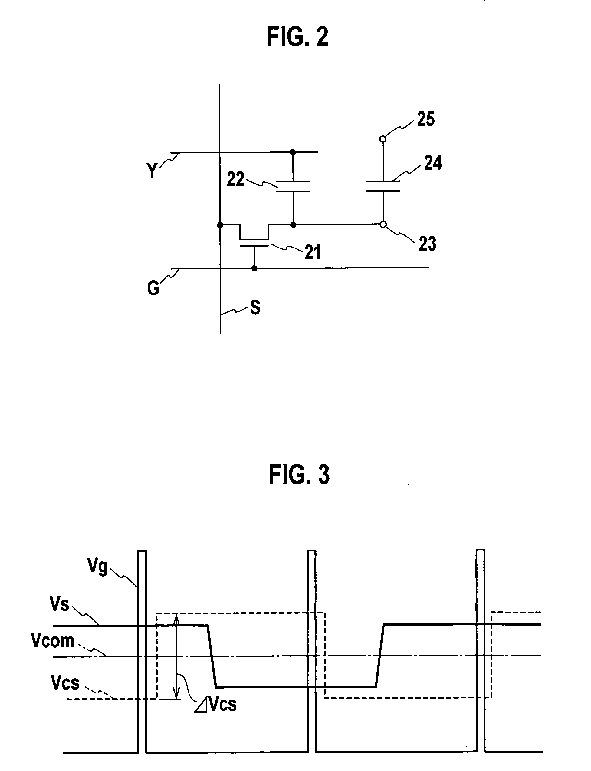
[0049] In the display section 2, a plurality of scan lines and a plurality of signal lines are routed so as to intersect each other. A pixel is placed for each of segments bordered by the scan lines and the signal lines. As shown in the circuit diagram of FIG. 2, each pixel includes a switch element 21, an auxiliary capacitance 22, a pixel electrode 23, a liquid crystal capac...
second embodiment
[0069] As shown in the schematic block diagram of FIG. 7, in a liquid crystal display device of a second embodiment, an array substrate 100 includes the display section 2, an auxiliary capacitance detector 30, an auxiliary capacitance voltage adjuster 40, and a power supply circuit 50 on a translucent substrate. In order to enable transistors of each circuit to be formed on the translucent substrate, thin-film transistors (TFT) are employed as the transistors of each circuit. The basic configuration of the display section 2 is similar to that of the first embodiment.
[0070] Next, a description will be given of the layer structures of a MOS thin-film transistor constituting the switch element 21 and the auxiliary capacitance 22. As shown in the cross-sectional view of FIG. 8, an nMOS thin-film transistor SWa, a pMOS thin-film transistor SWb, and the auxiliary capacitance 22 have layer structures including gate insulating films 71 of the same thickness. Specifically, a channel 70 made...
third embodiment
[0095] As shown in the schematic block diagram of FIG. 17, in a liquid crystal display device of a third embodiment, the auxiliary capacitance detector 30 further includes a second oscillator 31′, a second frequency counter 32′, a second register 33′, and a difference calculator 34. Other components are similar to those of the second embodiment, and therefore will not be further described here. It should be noted that, in this embodiment, the oscillator 31, the frequency counter 32, and the register 33 of the modified example shown in FIG. 13 in the second embodiment are referred to as a first oscillator 31, a first frequency counter 32, and a first register 33, respectively.
[0096]FIG. 18 is a circuit diagram showing the circuit configuration of the second oscillator 31′. The configuration of the second oscillator 31′ is basically the same as that of the first oscillator 31. However, the second oscillator 31′ includes a reference capacitance 27 having a structure different from tha...
PUM
 Abstract
Description
Claims
Application Information