Decoding circuit for memory device

Active Publication Date: 2005-03-24
SK HYNIX INC
View PDF5 Cites 4 Cited by
  • Summary
  • Abstract
  • Description
  • Claims
  • Application Information

AI Technical Summary

Benefits of technology

[0017] Another object of the present invention is to prevent a peak current from being flown in a semiconductor device as the decoded result for an undefined value, as aforementioned, has a specific value.
[0018] The other object of the present invention is to stabilize an operation of a semiconductor device and prevent a peak current from being flown in a semiconductor device by making a decoded result for an undefined value become a specific value, in a decoding operation for performing CL function and tWR function.

Problems solved by technology

In response to this, it can't be checked for an operational condition of a memory device as well.
In response to this, it can't be checked for an operational state of a memory device as well.
As aforementioned, in case that an address signal which is not defined for CL or tWR is generated, the conventional decoding circuit for a memory device causes a mis-operation in a memory device.

Method used


Image

  • Decoding circuit for memory device
  • Decoding circuit for memory device
  • Decoding circuit for memory device

Examples


Embodiment Construction

[0028] Reference will now be made in greater detail to a preferred embodiment of the invention, an example of which is illustrated in the accompanying drawings. Wherever possible, the same reference numerals will be used throughout the drawings and the description to refer to the same or like parts.

[0029] Hereinafter, it will be described about preferred embodiments of the present invention in detail with reference to the drawings.

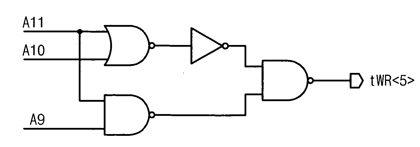
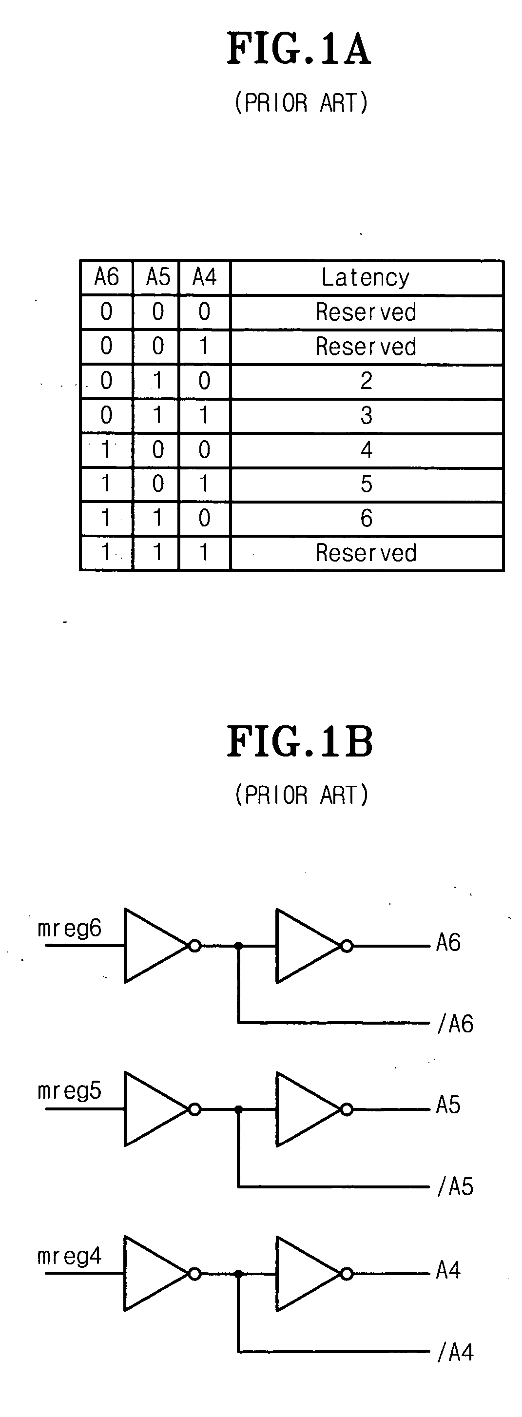
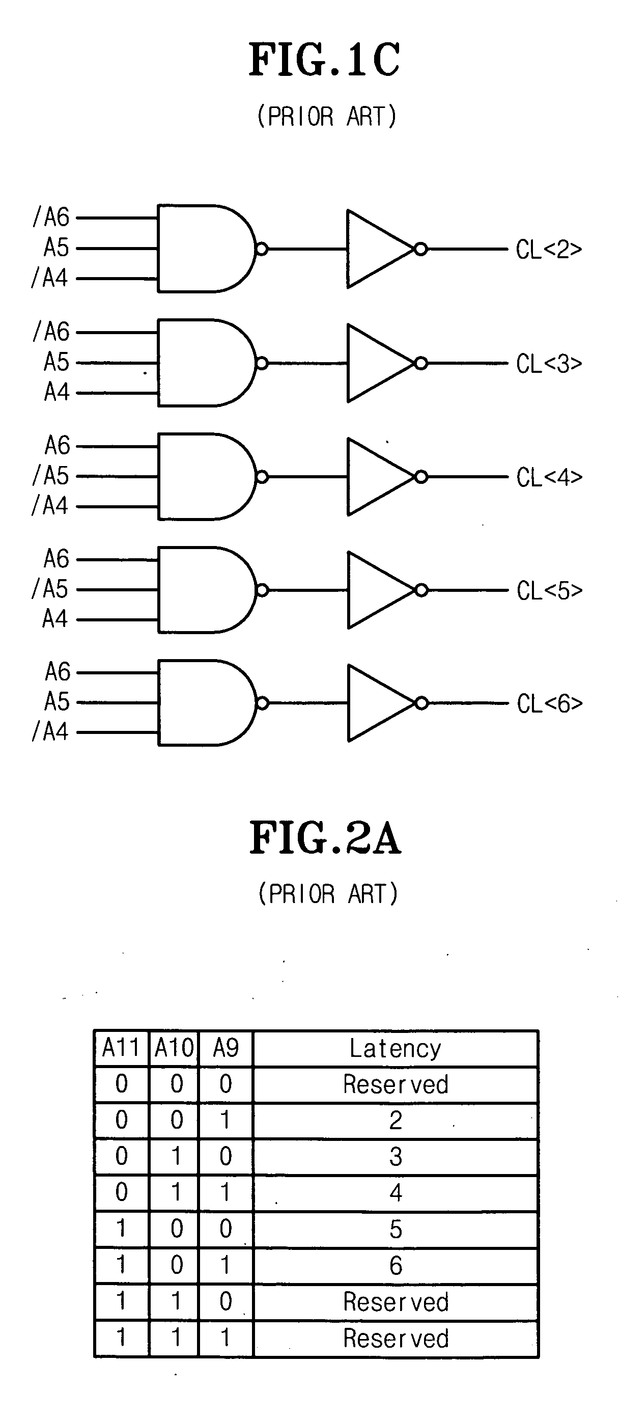
[0030] A decoding circuit for a semiconductor device in accordance with the present invention is schemed to decode an output to have a specific value when an undefined address signal is inputted.

[0031] For the scheme, address signals applied to the decoding circuit for the semiconductor device are divided into a first group corresponding to a defined result value and a second group corresponding to an undefined result value. The decoding circuit is comprised of a first logical circuit for outputting a result value defined by logically-combining the addr...


PUM


Abstract

Provided is a decoding circuit for a memory device which is improved in an operation of chip so as to enable the operation to be predictable by making a decoded result corresponding to an undefined code get a specific value. The decoding circuit for a memory device generates address signals by control signals set with a mode, and comprises a first logical circuit for decoding and outputting a result value defined by logically-combining the address signals corresponding to a first group and a second logical circuit for performing a decoding operation to have address signals with a specific value included in the defined result value by logically-combining address signals corresponding to a second group, by dividing the address signals into the first group corresponding to at least one defined result value and the second group corresponding to an undefined result value.

Description

BACKGROUND OF THE INVENTION [0001] 1. Field of the Invention [0002] The present invention relates to a decoding circuit, and more particularly to, a decoding circuit for a memory device, which is improved in an operation of chip so as to enable the operation to be predictable by making a decoded result corresponding to an undefined code become a specific value. [0003] 2. Description of the Related Art [0004] Generally, a memory device such as SRAM, DRAM, and a Flash memory is comprised of a decoding circuit which defines a control signal—for instance, CAS Latency(namely, CL) or Write recovery time(namely, tWR)—for setting an internal operation of the memory device by receiving an address signal. For reference, CL denotes the minimum number of clocks from inputting a column address to outputting data, and tWR denotes time from writing data in a cell to precharging the data. [0005] For instance, a decoding circuit applied to CL combines an address signal applied through the fourth, fi...

Claims


Application Information

Patent Timeline
IPC IPC(8): G11C5/06G11C8/10
CPCG11C8/10
Inventor AN, YONG BOK
Owner SK HYNIX INC
Why Eureka
Try Eureka