In-situ monitor of process and device parameters in integrated circuits

a technology of process and device parameters, applied in the direction of electronic circuit testing, measurement devices, instruments, etc., can solve the problems of inability to meet the critical dimensions of integrated circuits, and inability to meet the requirements of process conditions

Inactive Publication Date: 2009-09-22
INTEGRATED DEVICE TECH INC
View PDF29 Cites 66 Cited by
  • Summary
  • Abstract
  • Description
  • Claims
  • Application Information

AI Technical Summary

Problems solved by technology

In particular, test structures formed on test wafers are not always equivalent to the structures utilized in the integrated circuits.
Test wafers are often produced with abbreviated process conditions and often lack the critical dimensions utilized in the integrated circuits on wafers that are supposedly being tested.
Access to test wafer information can be expensive in both labor and material cost.
No direct method of determining some of these parameters on a specific die is generally available.
Current manufacturing technologies with 16 Å of gate oxide, however, have shown measured leakages of about 4×10⁻⁸ amperes per square micron with a bias voltage of about one volt.
The increase in device leakage with die sizing remaining the same adds to the increase in chip power consumption and design restrictions for scaled processes.
Previously, chip power consumption consisted primarily of the charging and discharging of internally and externally connected capacitance.
The leakage value may be excessive, representing single defects in the large area capacitor of the die independent of the test monitor.
There is a large variation in leakage currents from wafer to wafer and from batch to batch as a result of variations in defect levels and process conditions.
Therefore, utilizing a whole wafer to provide leakage current and extrapolating that data over each integrated circuit in a batch of wafers is often unreliable and misleading.
Product reliability is often associated with single defect failures.
Current products processed with thin gate oxides have witnessed increases in power consumption, thus increasing the temperature of the chip and thereby degrading speed performance.
These MOS devices are not necessarily representative of gate structures actually found on integrated circuits.
Consequently, values of leakage currents obtained by these test structures are not necessarily representative of the actual leakage current exhibited by devices produced by the technology.
The reliability of devices suffers as a result of thin gate oxides.
Reliability testing, or “burn-in,” is expensive both in labor and equipment costs.
Failures may occur from other than increases in gate oxide leakage, in which case it can be difficult to identify failure modes.

Method used


Image

  • In-situ monitor of process and device parameters in integrated circuits
  • In-situ monitor of process and device parameters in integrated circuits
  • In-situ monitor of process and device parameters in integrated circuits

Examples


Embodiment Construction

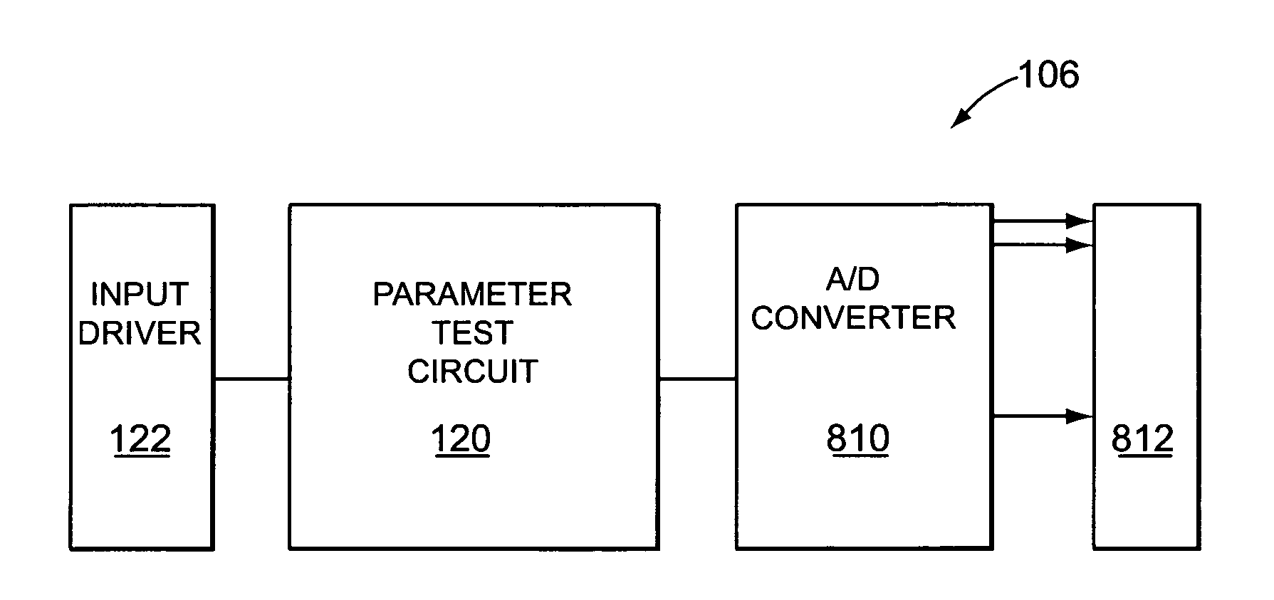
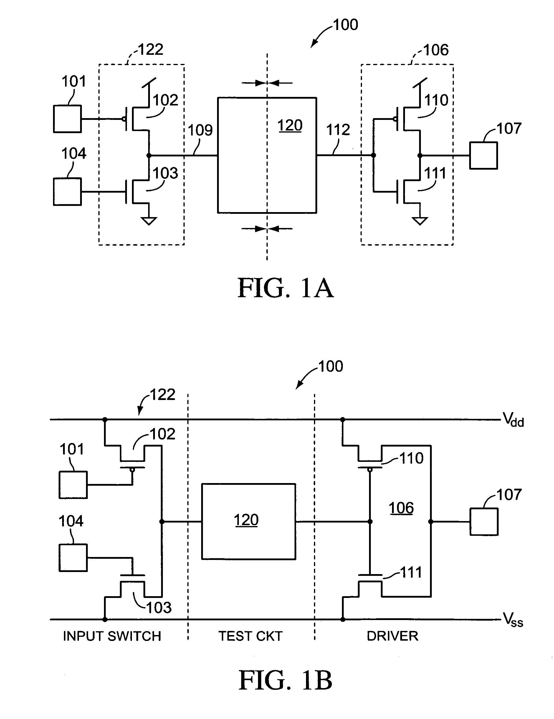
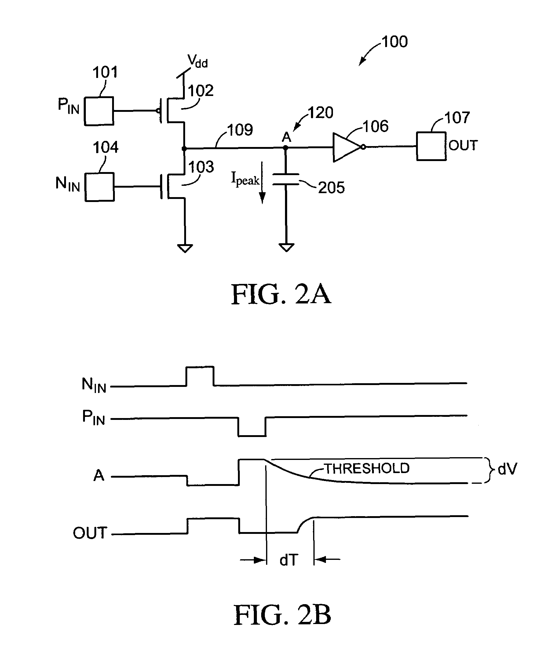
[0039]In accordance with embodiments of the present invention, circuits to measure process, design, and circuit parameters can be accessible at all stages of development and use of the integrated circuit chip in which they are embedded. Embodiments of the invention can range from a method of obtaining gate leakage data with a custom designed circuit, which may require special access pads, to a circuit for obtaining a full range of all process, device and circuit parameters incorporated in an existing scan path test system (JTAG) present in the integrated circuit. Therefore, in accordance with some embodiments of the present invention, scan path technology can be expanded from pin continuity testing and internal chip logic testing to process, device, and circuit parameter testing and monitoring.

[0040]Some embodiments of the invention can utilize additional bonding pads and separate testing resources, which may also require additional layout resources. However, some embodiments of the...


PUM


Abstract

In accordance with the invention, a testing circuit formed on the integrated circuit is presented. A testing circuit according to the present invention is coupled to a scan path circuit and includes an input circuit coupled to a parameter testing circuit and an output driver coupled to the parameter testing circuit. Embodiments of the parameter testing circuit can include circuits for testing process, device, and circuit characteristics of the integrated circuit. Further, some embodiments of the testing circuit can be included in a scan path system where sequences of various testing circuits are included. Further, test parameters obtained from the parameter testing circuits can be utilized to adjust operating parameters of the integrated circuit.

Description

RELATED APPLICATION[0001]This disclosure is a continuation-in-part of U.S. Pat. No. 11 / 064,038, filed Feb. 22, 2005 (now pending), which is herein incorporated by reference in its entirety.FIELD OF THE INVENTION[0002]The present invention is related to in-situ monitoring of semiconductor circuits and, in particular, to in-situ monitoring of process and device parameters in integrated circuits.BACKGROUND OF THE INVENTION[0003]Technology is trending toward the development of smaller and higher performance integrated circuits. The assessment of device parameters from test wafers that accompany batches of wafers in processing can be wholly misleading as to the geometries that actually exist on individual integrated circuits and even on the individual wafers that contain the integrated circuits. Tests that are conventionally performed on test wafers can include, for example, process, continuity, and design rule checks as well as device charateristic tests (e.g., device leakage tests), ga...

Claims


Application Information

Patent Timeline
Patent Type & Authority Patents(United States)
IPC IPC(8): G01R31/28G01R31/08
CPCG01R31/2853G01R31/2882G11C29/48G01R31/318555G11C29/1201G01R31/318541
Inventor PILLING, DAVID J.
Owner INTEGRATED DEVICE TECH INC
Why Eureka
Try Eureka