
Hierarchical layout method for integrated circuits

a layout method and integrated circuit technology, applied in the field of computer-aided design, can solve the problems of increasing data volume, affecting the design cycle time, design cost and time to market, and the complexity of these designs quadrupling every couple of years

Inactive Publication Date: 2002-12-19
IBM CORP
View PDF0 Cites 138 Cited by
  • Summary
  • Abstract
  • Description
  • Claims
  • Application Information

AI Technical Summary

Benefits of technology

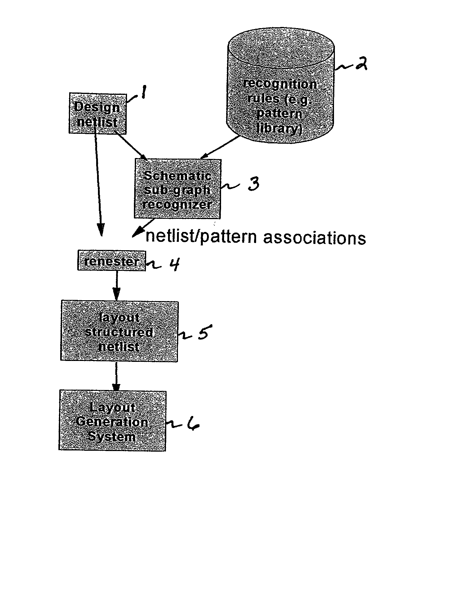
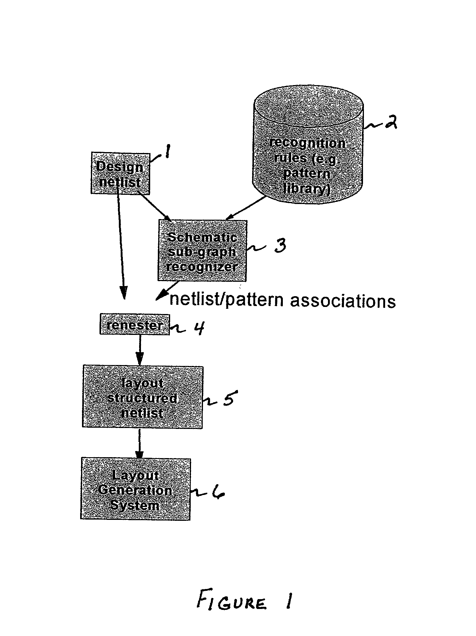
[0012] Renesting the schematic netlist by the pattern recognizer by initially creating a parameterized pattern library of the components used enables greater productivity in layout generation when compared to conventional manual transistor-level layout. The invention also facilitates in revisions of the layout that frequently occur in response to functional or performance tuning where iterations of preliminary designs are necessary. In addition, the invention aids the eventual migration of a design to subsequent generation of VLSI technology (e.g., from a 0.25 .mu.m process to a 0.18 .mu.m process).

Problems solved by technology

The complexity of these designs quadruples every couple of years.
This increasing data volume is becoming a significant problem for engineering design automation, since it stresses software design systems which in turn impact the design cycle time, design cost and time to market.
However, these hierarchically structured layouts are generated for preliminary analysis of the IC layout placement, and not as a final IC layout placement that is typically generated automatically prior to the optional routing and compacting processing.
As such, current placement layout methods require either manual layout which requires a great increase in effort relative to automated placement or generation of individual transistor layouts.
Such manual modification is labor intensive and error prone.
Use of a general placement present problems that include transistors being larger in size.
Also, it is more difficult to achieve an optimal design with general placement since automated transistor design tools are not as sophisticated as standard-cell based tools.
Further, there are other method or technical constraints posed by the general placement layout (e.g., embedded latches or SRAM cells are typically selected from a pre-existing library, rather than use of custom cells).
In summary, the above problems in connection with current placement layout methodologies are costly and time consuming.

Method used


Image

  • Hierarchical layout method for integrated circuits
  • Hierarchical layout method for integrated circuits
  • Hierarchical layout method for integrated circuits

Examples


Embodiment Construction

[0018] The present invention provides a method for integrated circuit (IC) design layout generation. A physical design is a set of mask shapes that denote the design of an integrated circuit. Within the physical design, a shape is a planar set of points and the bounding edges they define. The physical design of an integrated circuit is expressed in the form of a hierarchical layout, which consists of duplicate instances of basic design components connected together to form a complex design. The hierarchical layout characterizes the design as nested data, where design components are retained embedded as much as possible in the design. In contrast to nested data, flat or flattened design data has all of its shapes transformed to the highest level of the design, and thus expressed in a non-hierarchical flat form. The invention described below automates the nesting process by applying recognition rules to the non-hierarchical, flat layout to automatically modify the flat layout into a c...


PUM


Abstract

A method for hierarchical layout of an electronic design using an electronic computer aided design system, wherein the method includes generating a parameterized pattern library and using an existing netlist and analyze in a pattern recognizer, from which a list of associations between the pattern library and the netlist is created. Renesting then occurs wherein the netlist using the list of associations is used for generating a hierarchical layout of the electronic components in the design.

Description

[0001] 1. Field of the Invention[0002] The present invention generally relates to computer-aided design and in particular to a hierarchical layout method for integrated circuits.[0003] 2. Description of the Related Art[0004] All integrated circuits and their physical packaging are described by physical designs in the form of hierarchical two-dimensional geometric models. Hierarchical characterization is typically used to define the wiring channels and connection ports that can be used to route wire over a design partition in the higher level cell. The complexity of these designs quadruples every couple of years. This increasing data volume is becoming a significant problem for engineering design automation, since it stresses software design systems which in turn impact the design cycle time, design cost and time to market.[0005] The input to the physical design problem is a circuit diagram, and the output is generating a layout of the integrated circuit. Well-known techniques for im...

Claims


Application Information

Patent Timeline
Patent Type & Authority Applications(United States)
IPC IPC(8): G06F17/50
CPCG06F17/5068G06F30/39
Inventor ALLEN, ROBERT J.COHN, JOHN M.LOVEJOY, STEVE G.
Owner IBM CORP
Learn More