
Integrated circuits having post-silicon adjustment control

a post-silicon adjustment and integrated circuit technology, applied in the direction of instruments, heat measurement, digital computer details, etc., can solve the problems of power consumption problem, loss of performance improvement generation, and difficulty in precisely manufacturing chips, so as to improve power consumption or program execution speed, double the program execution time, and reduce power consumption per second

Inactive Publication Date: 2005-10-18
RPX CORP
View PDF7 Cites 132 Cited by
  • Summary
  • Abstract
  • Description
  • Claims
  • Application Information

AI Technical Summary

Benefits of technology

[0006]The paper, “Effectiveness of Adaptive Supply Voltage and Body Bias for Reducing Impact of Parameter variations in Low Power and High Performance Microprocessors,” by James W. Tschanz, etal., IEEE Journal of Solid-State Circuits, VOL. 38, No.5, May, 2003, shows that controlling the adaptive supply voltage and the body bias is effective in overcoming problems with those parameter variations.
[0009]In U.S. Pat. No. 5,996,083, the rate of program execution is controlled by software that changes the data bus width and the power latency values. The power consumption per second can be decreased by changing the data bus width from 64 bits to 32 bits, but this approximately doubles the program execution time. The execution time for each program is determined by the clock rate and the power latency, which is the time required to change the applied voltage or the status condition (e.g., standby or execute). The power latency time is needed to stabilize the applied power and the program execution and it adds to the total consumption of power and the total operation speed. Changes in data bus width and power latency are controlled by the instruction program. In U.S. Pat. No. 5,996,083, the power consumption or program execution speed is improved by changing the program using an internal control circuit.

Problems solved by technology

Manufacturing chips that precisely is difficult due to variations in threshold voltages, the resistance of wires, and the capacitance of lines.
This paper predicts that when 50 nm technology is employed, a generation of performance improvements may be lost due to systematic within-die fluctuations.
Another difficulty is the power consumption problem.
Million or gigascale integration requires a huge power consumption.
Thus, there are problems in IC chips with parameter fluctuations and extreme operating temperatures, as well as local parameter fluctuations and internal thermal distributions.

Method used


Image

  • Integrated circuits having post-silicon adjustment control
  • Integrated circuits having post-silicon adjustment control
  • Integrated circuits having post-silicon adjustment control

Examples


Embodiment Construction

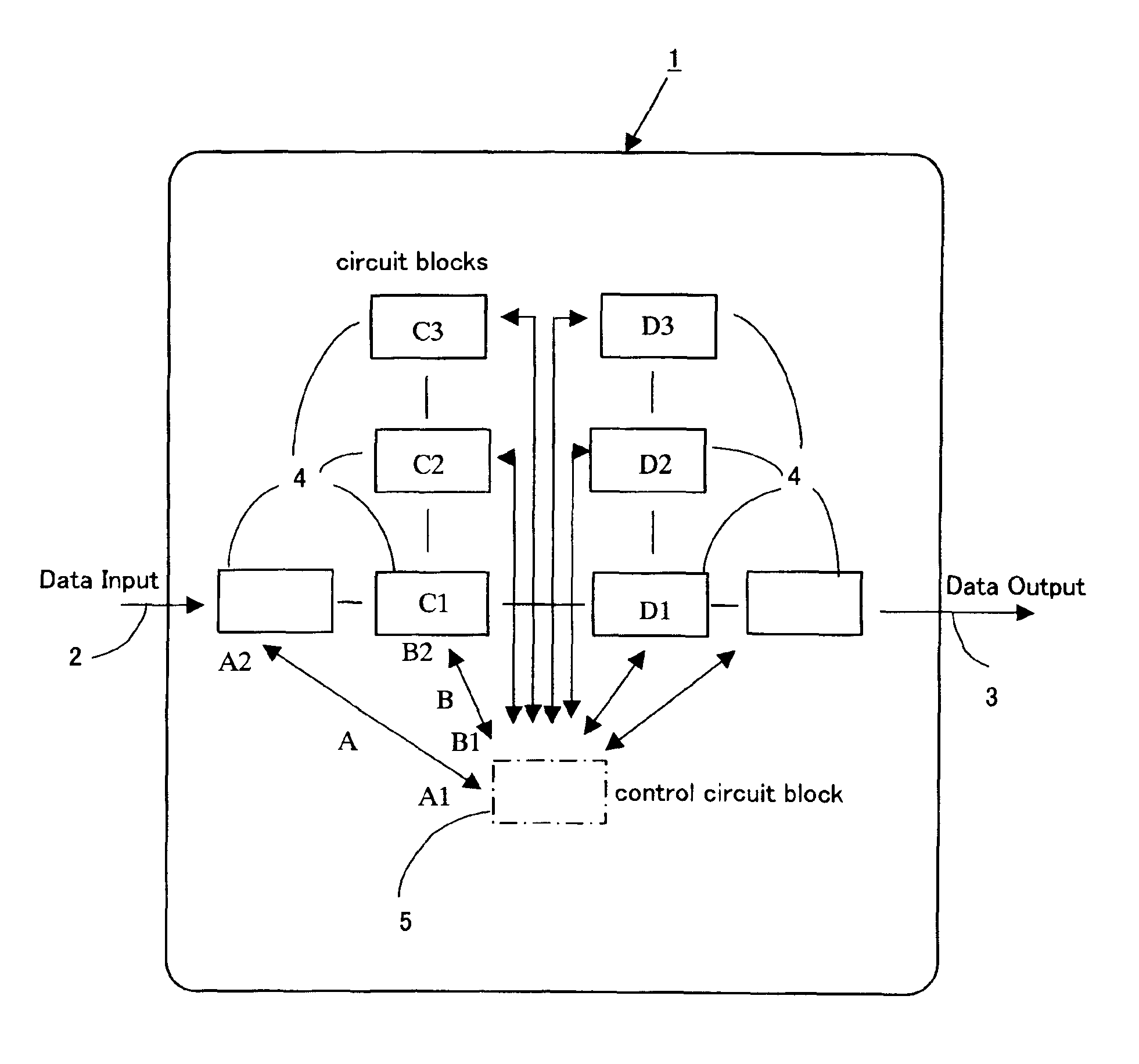
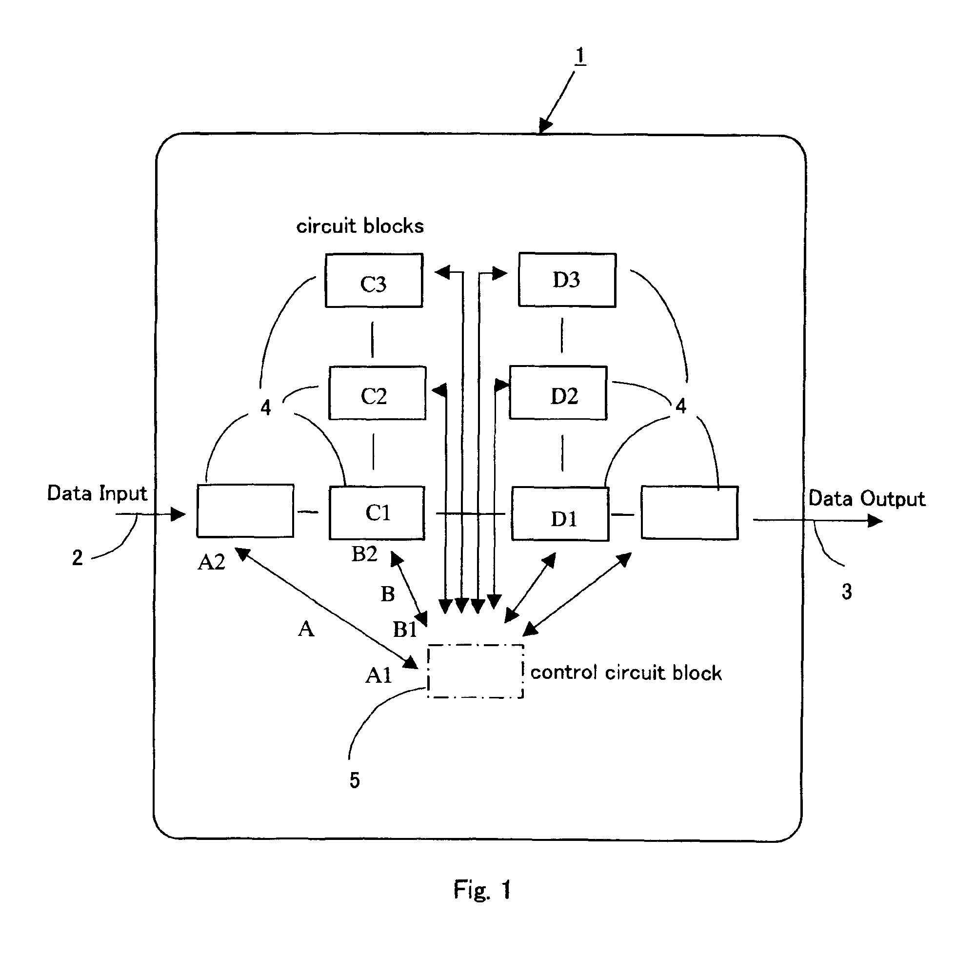
[0019]In FIG. 1, large scale integrated circuit (LSI) chip 1, either as one of many IC chips on a wafer or as an assembled individual IC chip, has a data input 2 and a data output 3. Chip 1 comprises numerous partitioned circuit blocks 4, each of which has an internal temperature monitor circuit, or some temperature-generating or temperature-sensitive blocks have such monitors, but the temperature monitor circuit could also comprise a single circuit block 4. Control circuit block 5 controls various parameters of circuit blocks 4, such as clock speed, operation clock speed, supply voltage, and body-bias voltage.

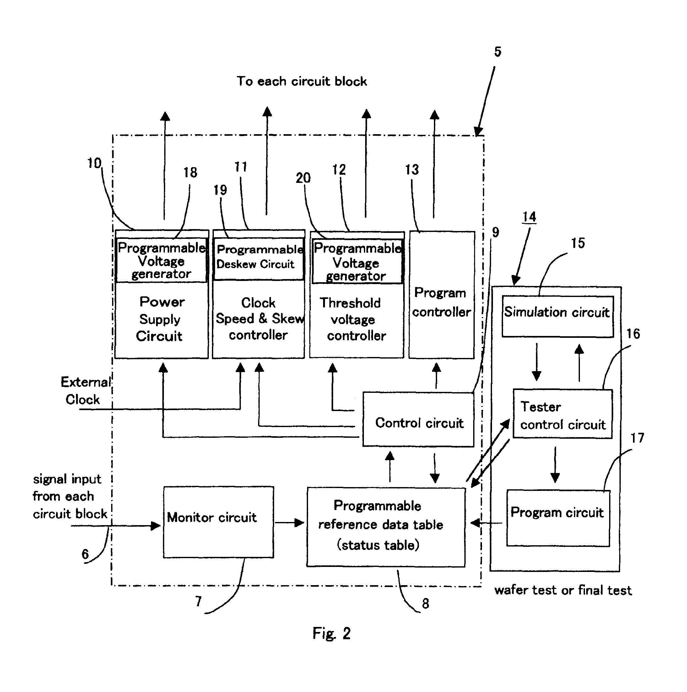
[0020]In FIG. 2, signal input 6 from each circuit block 4 contains information such as whether a circuit block is operating or is on stand-by, the temperature of the circuit block and, if it is operating, at what clock speed it is operating and / or what program it is executing. Signal input 6 goes to monitor circuit 7, which determines which circuit blocks will be used next and...


PUM


Abstract

An integrated circuit system has a reference data table for holding information that is used to control at least one circuit block in the system and also has a power supply circuit, a body bias control circuit, a clock delivery circuit, a temperature monitor circuit, and / or a configuration control circuit. The performance of the system is improved by obtaining system performance data by testing the system at different supply voltages, different body-bias voltages, different clock speeds, and / or different temperatures. Values based on the data are entered into the reference data table. The power supply circuit, the body bias control circuit, the clock delivery circuit, and / or the temperature monitor circuit data is adjusted using the entered values.

Description

[0001]This application is a continuation-in-part of application Ser. No. 10 / 063,450, filed Apr. 24, 2002 now U.S. Pat. No. 6,792,379, titled “Data-Based Control of Integrated Circuits.”BACKGROUND OF INVENTIONSummary of Invention[0002]This invention relates the use of data obtained by testing integrated circuit (IC) chips to control the performance of the IC chip. In particular, it relates to simulating the operation of an integrated circuit chip and programming the reference data table of the chip with information based on data obtained from that simulation.[0003]Integrated circuit (IC) chips are being required to have higher execution speeds and better performances. In order to meet such requirements, IC chips having a million or more transistors are placed on a die. This requires that narrower dimensions, such as 130 nm or less, must be used. Manufacturing chips that precisely is difficult due to variations in threshold voltages, the resistance of wires, and the capacitance of lin...

Claims


Application Information

Patent Timeline
Patent Type & Authority Patents(United States)
IPC IPC(8): G01R27/00G01R27/28G01R31/00G06F19/00G01R31/317G01R31/319G16Z99/00
CPCG01R31/31707G01R31/319G16Z99/00G01R31/00G01R27/28
Inventor ANDO, YOSHIYUKI
Owner RPX CORP
Learn More