Check patentability & draft patents in minutes with Patsnap Eureka AI!

Photoresist composition and method of manufacturing a thin-film transistor substrate using the same

a technology of thin-film transistors and compositions, applied in the direction of photosensitive materials, instruments, photomechanical equipment, etc., can solve the problems of short circuit or pixel defect, decrease the aperture ratio of display devices, and increase the skew of display devices, etc., to achieve efficient application

Inactive Publication Date: 2009-09-29
SAMSUNG DISPLAY CO LTD
View PDF9 Cites 25 Cited by
  • Summary
  • Abstract
  • Description
  • Claims
  • Application Information

AI Technical Summary

Benefits of technology

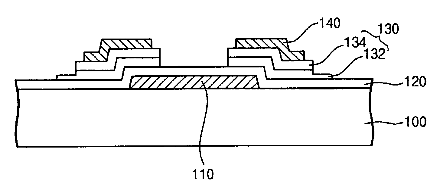
[0011]Therefore, a halftone photoresist film may be stably formed through a slit exposure process using the photoresist composition. Thus, a negative photoresist film may be efficiently applied to a method of manufacturing a TFT substrate using four masks.
[0012]Accordingly, with the methods of manufacturing a TFT substrate in accordance with exemplary embodiments of the present, a TFT substrate manufacturing process is provided in which a TFT substrate may be stably formed, and which also has the benefits associated with using a negative photoresist film.

Problems solved by technology

However, when a photoresist film is formed using a positive photoresist composition, the residual uniformity of the photoresist film corresponding to a channel portion may be poor, thereby resulting in a short circuit or a pixel defect.
Furthermore, with the above mentioned conventional positive photoresist composition, a semiconductor layer may excessively protrude beneath source-drain electrodes, to decrease the aperture ratio of a display device.
Consequently, skew may also be increased when etching processes are performed two or more times.
However, conventional negative photoresist compositions have relatively high contrast so that forming a halftone photoresist film by slit exposure may be difficult.

Method used


Image

  • Photoresist composition and method of manufacturing a thin-film transistor substrate using the same
  • Photoresist composition and method of manufacturing a thin-film transistor substrate using the same
  • Photoresist composition and method of manufacturing a thin-film transistor substrate using the same

Examples


example 1

[0043]About 400 g of propylene glycol methyl ether propionate as a solvent, about 100 g of meta-cresol / formaldehyde novolak resin, of which molecular weight is about 6,000 [weight-average molecular weight (Mw) / number-average molecular weight (Mn)=1.69] as a novolak resin, about 10 g of hexamethylolmelamine hexamethyl ether as a cross-linker, about 3.0 g of diphenyliodonium trifluoromethane sulfonate as a photo-acid generator, about 0.6 g of UV yellow 1549 as an azo-based dye and about 1.0 g of trioctylamine as an amine additive were mixed to prepare a photoresist composition.

example 2

[0044]About 400 g of propylene glycol methyl ether propionate as a solvent, about 100 g of meta-cresol / formaldehyde novolak resin, of which molecular weight is about 7,000 [weight-average molecular weight (Mw) / number-average molecular weight (Mn)=1.71] as a novolak resin, about 8.0 g of hexamethylolmelamine hexamethyl ether as a cross-linker, about 4.0 g of triazine as a photo-acid generator, about 1.0 g of UV yellow 1549 as an azo-based dye and about 1.0 g of trioctylamine as an amine additive were mixed to prepare a photoresist composition.

example 3

[0045]About 400 g of propylene glycol methyl ether propionate as a solvent, about 100 g of meta-cresol / formaldehyde novolak resin, of which molecular weight is about 8,000 [weight-average molecular weight (Mw) / number-average molecular weight (Mn)=1.74] as a novolak resin, about 12 g of hexamethylolmelamine hexamethyl ether as a cross-linker, about 5.0 g of triazine as a photo-acid generator, about 1.5 g of UV yellow 1549 as an azo-based dye and about 1.0 g of trioctylamine as an amine additive were mixed to prepare a photoresist composition.


PUM

PropertyMeasurementUnit
taper angleaaaaaaaaaa
temperatureaaaaaaaaaa
anglesaaaaaaaaaa

Abstract

A photoresist composition includes about 10 to about 70% by weight of a binder resin including a phenol-based polymer, about 0.5 to about 10% by weight of a photo-acid generator, about 1 to about 20% by weight of a cross-linker, about 0.1 to about 5% by weight of a dye and about 10 to about 80% by weight of a solvent. The photoresist composition may be applied to, for example, a method of manufacturing a TFT substrate.

Description

CROSS-REFERENCE TO RELATED APPLICATIONS[0001]This application relies for priority upon Korean Patent Application No. 2005-77308 filed on Aug. 23, 2005, the contents of which are hereby incorporated by reference herein in their entirety.BACKGROUND OF THE INVENTION[0002]1. Technical Field[0003]The present disclosure relates to a photoresist composition and a method of manufacturing a thin-film transistor substrate using the photoresist composition. More particularly, the present disclosure relates to a photoresist composition capable of forming a halftone photoresist film and a method of manufacturing a thin-film transistor substrate using the photoresist composition.[0004]2. Description of the Related Art[0005]A positive photoresist composition may be used for manufacturing a thin-film transistor (TFT) substrate using four masks. However, when a photoresist film is formed using a positive photoresist composition, the residual uniformity of the photoresist film corresponding to a chan...

Claims


Application Information

Patent Timeline
Patent Type & Authority Patents(United States)
IPC IPC(8): G03F7/00G03F7/004
CPCG03F7/0382G03F7/105H01L21/32139H01L29/78669H01L29/66765Y10S430/114Y10S430/106G03F7/0045
Inventor PARK, JEONG-MINLEE, HI-KUKYOUN, HYOC-MINKOO, KI-HYUKKIM, BYUNG-UK
Owner SAMSUNG DISPLAY CO LTD
Features
  • R&D
  • Intellectual Property
  • Life Sciences
  • Materials
  • Tech Scout
  • Unparalleled Data Quality
  • Higher Quality Content
  • 60% Fewer Hallucinations
Learn More