A drawback of such detectors however is their inability to provide data or feedback as to the number and / or energy of photons detected.
While it is generally recognized that CT imaging would not be a viable diagnostic imaging tool without the advancements achieved with conventional CT detector design, a drawback of these detectors is their inability to provide energy discriminatory data or otherwise count the number and / or measure the energy of photons actually received by a given detector element or pixel.
Under the charge integration operation mode, the photodiode is not capable of discriminating between the energy level or the photon count from the scintillation.
Such detectors have large detector elements and as such are not readily adapted to CT applications requiring high resolution imaging to capture anatomical detail in the imaged object.
A drawback of direct conversion semiconductor detectors, however, is that these types of detectors cannot count at the x-ray photon flux rates typically encountered with conventional CT systems, e.g. at or above 5-100 million counts per sec per millimeter squared (Mcps).
The very high x-ray photon flux rate, above 5-100 Mcps, causes pile-up and polarization which ultimately leads to detector saturation.
Above these thresholds, the detector response is not predictable or has degraded dose utilization.
For SPECT and PET, imaging flux levels are below 5-100 Mcps and such saturation in a semiconductor detector for SPECT and PET is not a practical concern.
What can be problematic, however, is that the bowtie filter may not be optimal given that a subject population is significantly less than uniform and not exactly elliptical in shape.
Low x-ray flux in the projection will ultimately contribute to noise in the reconstructed image of the subject.
Detector saturation causes loss of imaging information and results in artifacts in x-ray projection and CT images.
In addition, hysteresis and other non-linear effects occur at flux levels near detector saturation as well as flux levels over detector saturation.
Direct conversion detectors are susceptible to a phenomenon called “polarization” where charge trapping inside the material changes the internal electric field, alters the detector count and energy response in an unpredictable way, and results in hysteresis where response is altered by previous exposure history.
Incomplete collection of x-rays results in reduced image quality, i.e. a noisy image, and poor utilization of dose to the imaged object.
However, there is a reliability issue to routing of high voltage signals.
This again results in poor dose utilization and image artifacts.
However, small pixel size results in higher cost and there are more channels per unit area which need to be connected to readout electronics.
This sharing of charge results in incomplete energy information and / or a miscount of x-ray photons because the readout electronics are not configured to combine simultaneous signals in neighboring pixels.
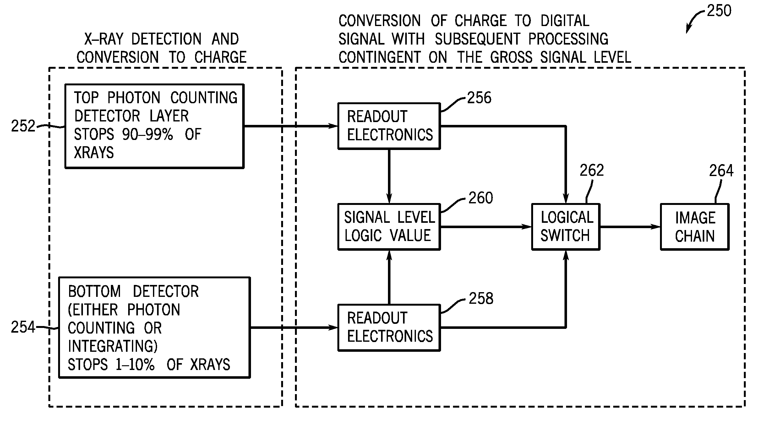
Very high flux rates are possible with thin, photon counting, direct conversion silicon layers with pixel size <0.1 mm, but there is not sufficient stopping power in these thin layers to stop the x-rays.
In the case of a photodiode, the electronic gain is not sufficient to overcome the electronic noise.
In the case of APDs, there is additional gain but with associated gain-instability noise, temperature sensitivity and reliability issues.
In the case of photomultiplier tubes, these devices are too large and costly for high resolution detectors covering large areas.
Detector saturation can affect image quality by constraining the number of photons used to reconstruct the image and introducing image artifacts.
For CT imaging, the reconstruction is not tolerant to missing or corrupted data.
The reconstruction of the data set with these uncorrected saturated values will cause severe artifacts in the image.
However, this solution leads to increased scanned time.
That is, there is a penalty that the acquisition time for the image is increased in proportion to the nominal flux needed to acquire a certain number of x-rays that meet image quality requirements.
In a typical imaging application, x-rays are absorbed in the direct conversion material which results in creation of an electrical charge in the direct conversion material.
One drawback of direct conversion semiconductor detectors, however, is that x-rays absorbed in the direct conversion material near the gaps or perimeters of the anodes can result in a charge being generated therein that is shared by at least two neighboring pixel anodes.
When using charge integration electronics, charge sharing can manifest itself as crosstalk between neighboring pixels, thus rendering the electronics susceptible to electronic noise amplification and spatially blurring of the image.
When using pulse counting electronics, charge sharing can result in dividing the charge between at least two anodes, resulting in lost counts when the amplitude of the charge pulse collected in at least one of the anodes is below a discrimination threshold.
Additionally, when pulse counting, high energy x-rays can result in loss of detection quantum efficiency (DQE) by the creation of two or more counts being collected in two or more neighboring anodes, thus mis-counting the events and binning for instance a single high energy event as two or more low-energy events.
Another drawback of direct conversion semiconductor detectors is that the response at the edge and corners of the direct conversion crystal may not be not reproducible.
The changing internal field can cause a poor detector response that can lead to image quality problems.
However, smaller pixel size can result in higher cost because there are more channels per unit area which need to be connected to readout electronics.
Because the perimeter is the region where a charge may be shared between two or more pixels, incomplete energy information and / or a miscount of x-ray photons occurs because the readout electronics are not configured to combine near-simultaneous signals in neighboring pixels.
However, such electronics can be costly and difficult to implement.
However, a guard ring does not prevent trapping of charge within the semiconductor and does not prevent a changing electric field from developing within the semiconductor.


