Method and system for reducing the time-to-market concerns for embedded system design

a technology of embedded systems and time-to-market concerns, applied in the field of reducing time-to-market concerns for embedded system design, can solve the problems of significant time incurred, devices are required to be small, low-power, light-weight and feature-rich, etc., and achieve the effect of reducing tim

Inactive Publication Date: 2009-11-17
NVIDIA CORP
View PDF74 Cites 17 Cited by
  • Summary
  • Abstract
  • Description
  • Claims
  • Application Information

AI Technical Summary

Benefits of technology

[0006]With the aspects of the present invention, supplementation of an existing infrastructure for an embedded system with individualized / proprietary functionality reduces the time needed to develop a signal processing product to meet a particular market need. Such time savings is of considerable value in the rapidly changing environment of the embedded system market. These and other advantages will become readily apparent from the following detailed description and accompanying drawings.

Problems solved by technology

Embedded systems face challenges in producing performance with minimal delay, minimal power consumption, and at minimal cost.
As the numbers and types of consumer applications where embedded systems are employed increases, these challenges become even more pressing.
By their nature, these devices are required to be small, low-power, light-weight, and feature-rich.
However, significant time in incurred as each design goes through the development process and reaches the market.

Method used


Image

  • Method and system for reducing the time-to-market concerns for embedded system design
  • Method and system for reducing the time-to-market concerns for embedded system design
  • Method and system for reducing the time-to-market concerns for embedded system design

Examples


Embodiment Construction

[0013]The present invention relates to reducing the time-to-market concerns for embedded system design. The following description is presented to enable one of ordinary skill in the art to make and use the invention and is provided in the context of a patent application and its requirements. Various modifications to the preferred embodiment and the generic principles and features described herein will be readily apparent to those skilled in the art. Thus, the present invention is not intended to be limited to the embodiment shown but is to be accorded the widest scope consistent with the principles and features described herein.

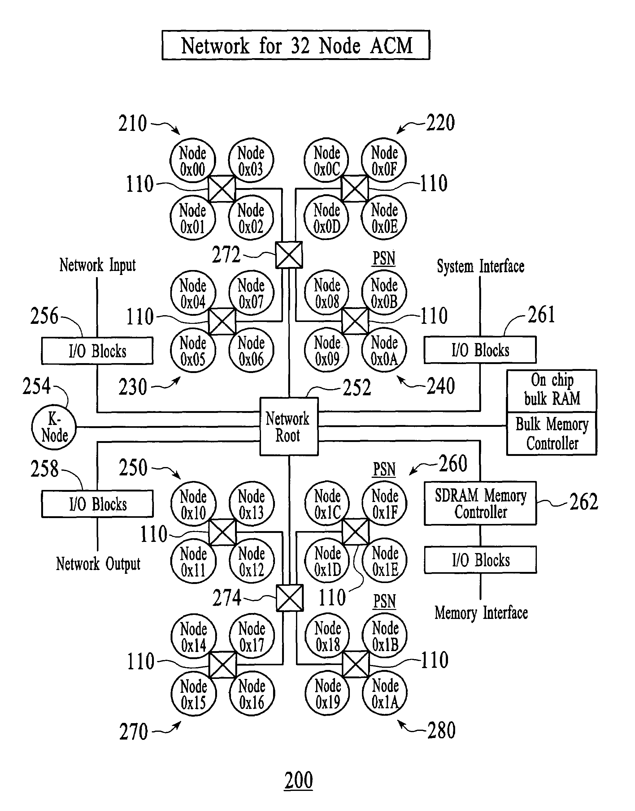
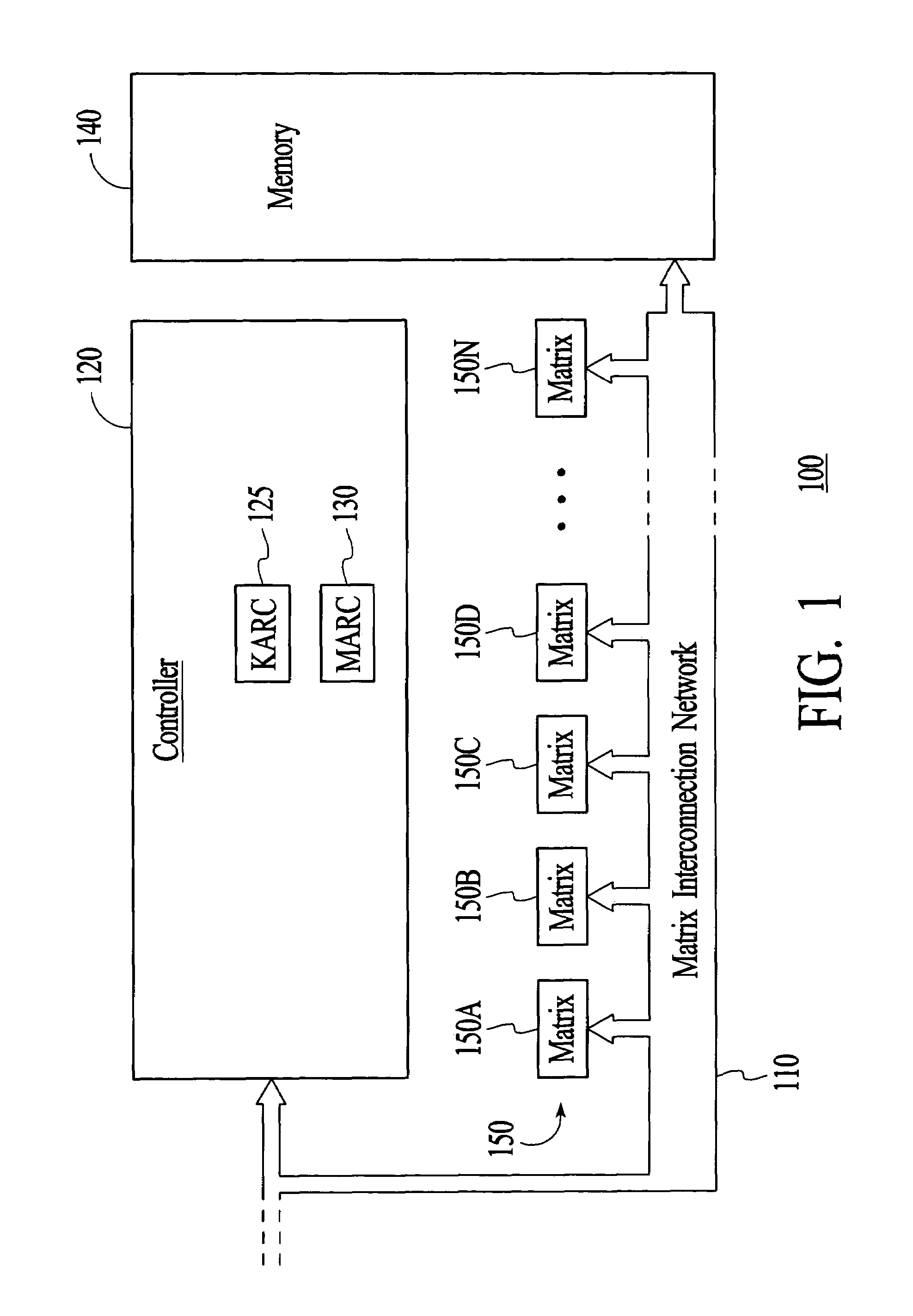
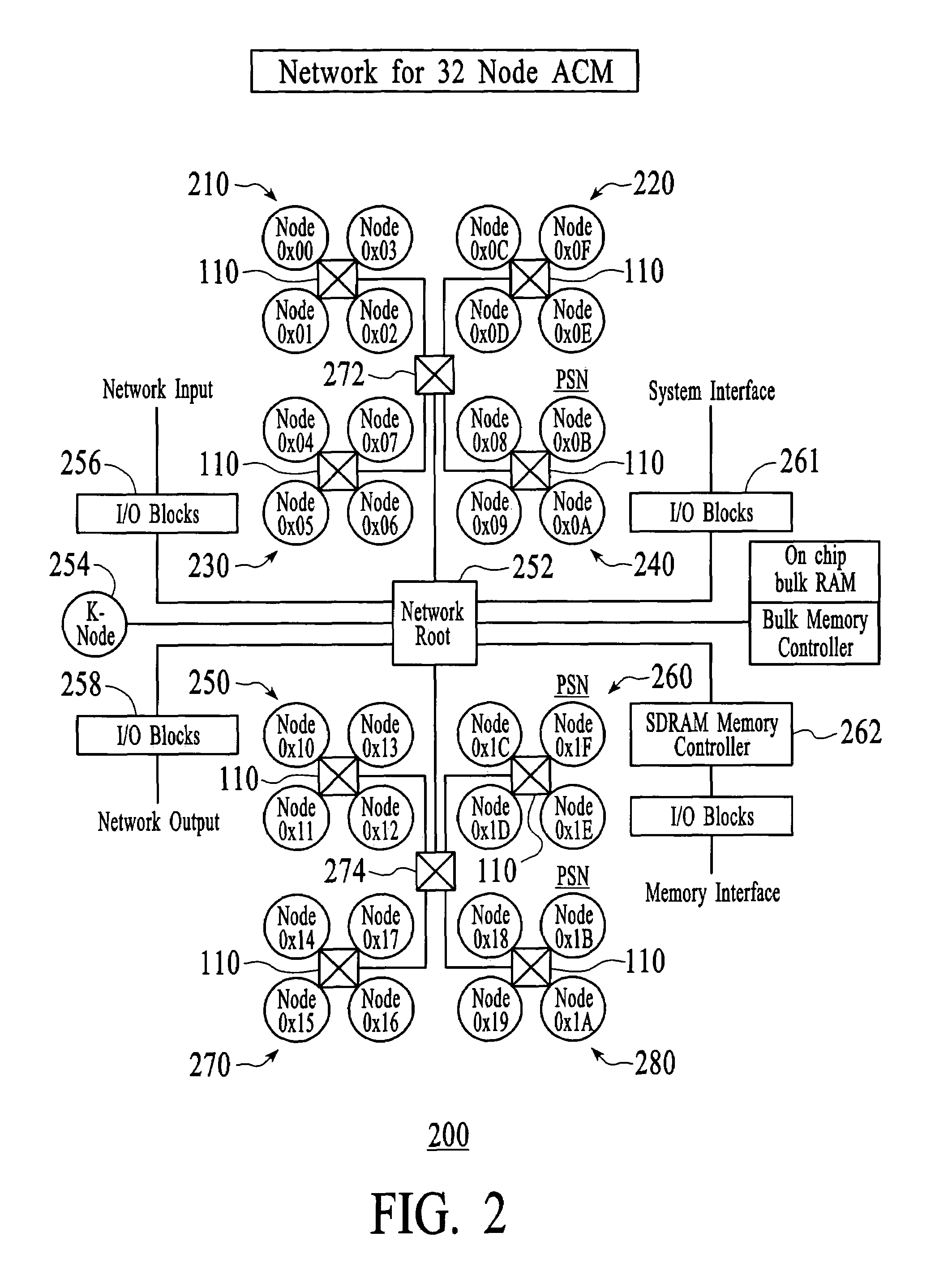
[0014]In order to reduce the time-to-market of an embedded system design / signal processing product, the present invention utilizes a homogeneous, scalable, extreme bandwidth network that connects heterogeneous nodes (computational elements), intelligent memory controllers, and configurable input / output ports and system bus interfaces, as described in co-pendi...


PUM


Abstract

Aspects for reducing the time-to-market concerns for embedded system design are described. The aspects include providing an infrastructure to support a plurality of heterogeneous processing nodes as a reconfigurable network. Further included is utilizing the infrastructure to customize at least one of the heterogeneous processing nodes according to individualized design needs to achieve a desired embedded system signal processing engine.

Description

CROSS-REFERENCE TO RELATED APPLICATION[0001]This application is claiming under 35 USC 119(e) the benefit of provisional patent application Ser. No. 60 / 388,249 filed on Jun. 12, 2002.FIELD OF THE INVENTION[0002]The present invention relates to reducing the time-to-market concerns for embedded system design.BACKGROUND OF THE INVENTION[0003]The electronics industry has become increasingly driven to meet the demands of high-volume consumer applications, which comprise a majority of the embedded systems market. Embedded systems face challenges in producing performance with minimal delay, minimal power consumption, and at minimal cost. As the numbers and types of consumer applications where embedded systems are employed increases, these challenges become even more pressing. Examples of consumer applications where embedded systems are employed include handheld devices, such as cell phones, personal digital assistants (PDAs), global positioning system (GPS) receivers, digital cameras, etc. ...

Claims


Application Information

Patent Timeline
Patent Type & Authority Patents(United States)
IPC IPC(8): G06F15/76
CPCG06F15/161
Inventor MASTER, PAUL L.SCHEUERMANN, W. JAMES
Owner NVIDIA CORP
Why Eureka
Try Eureka