Supercharge Your Innovation With Domain-Expert AI Agents!

Device for making an in-mold circuit

a technology of in-mold circuit and device, which is applied in the field of communication devices, can solve the problems of insufficient cost reduction, insufficient cost reduction, and mechanical process of chip bonding, and achieve the effect of slowing down and reducing throughpu

Inactive Publication Date: 2009-11-24
CHECKPOINT SYST INC
View PDF10 Cites 1 Cited by
  • Summary
  • Abstract
  • Description
  • Claims
  • Application Information

AI Technical Summary

Benefits of technology

The patent describes a method and device for making an in-mold circuit by embedding chips into a poly sheet and adding a conductive wire to form a connection with the chips. The poly sheet is heated and the chips and wire are embedded into the sheet simultaneously as they move through the machine direction. The method can also include separating the embedded conductive wire into portions with nonconductive gaps and creating conductive communication between the embedded circuit and wire. The invention allows for precise placement and connection of chips in a flexible and reheatable material.

Problems solved by technology

Chip bonding is costly.
While the increasing volume of the number of chips helps to drive the IC cost down, bonding is a mechanical process and does not benefit from the same technology advances or economic scale.
Current methods of chip bonding do not adequately address costs.
However, straps do not address the problem directly, as bonding is still required, but to a smaller tag.
However, such straps do not lend themselves to easy integration into flexible tags (e.g., RFID tags).
The standard bonding processes are all known strap-based solutions, and therefore less than ideal.
One related art attachment method, called Fluidic Self Assembly (FSA), provides insufficiently robust bonds.
Because the chips find their own way into bonding sockets, the chips cannot use adhesives or flux, since anything sticky prevents free motion of the chips into the sockets.
This flat-to-edge bond is different than and less reliable than traditional bonds, which are made flat-to-flat.
The FSA process is slow and uses multiple steps and requires a high degree of accuracy with known technology products available today.
Flip chip bonding, a current state of the art process, is expensive because of the need to match each chip to a tiny, precision-cut bonding site.
As chips get smaller, it becomes even harder to precisely cut and prepare the bonding site.
Retracing a path during the bonding process takes time, causes vibration, and wears mechanical linkages.
These linkages also create uncertainty in absolute position.
A problem exists with the current technology during chip placement onto a dipole.
Chips placed down on an antenna structure, such as an aluminum strap to form a bridge or RFID circuit, are easily cracked causing chip failure.
However, this solution does not cure the problem of chips cracking in the first place.

Method used


Image

  • Device for making an in-mold circuit
  • Device for making an in-mold circuit
  • Device for making an in-mold circuit

Examples


Embodiment Construction

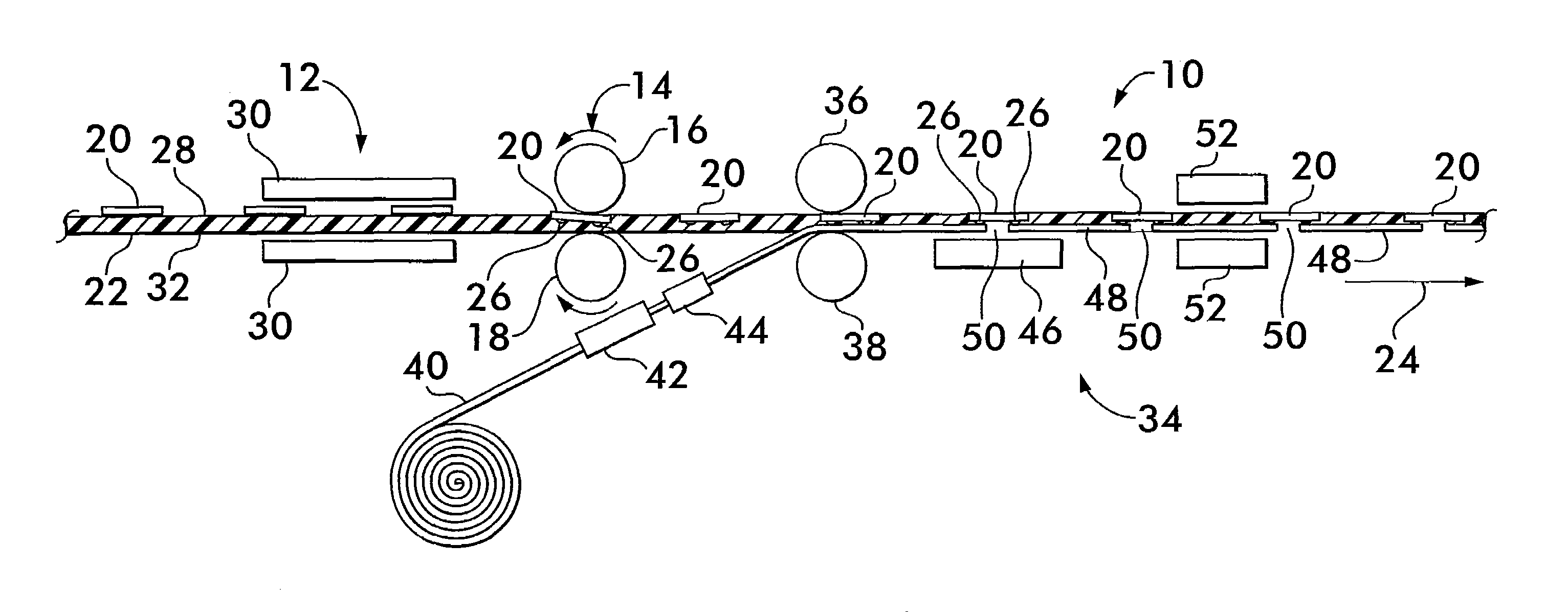
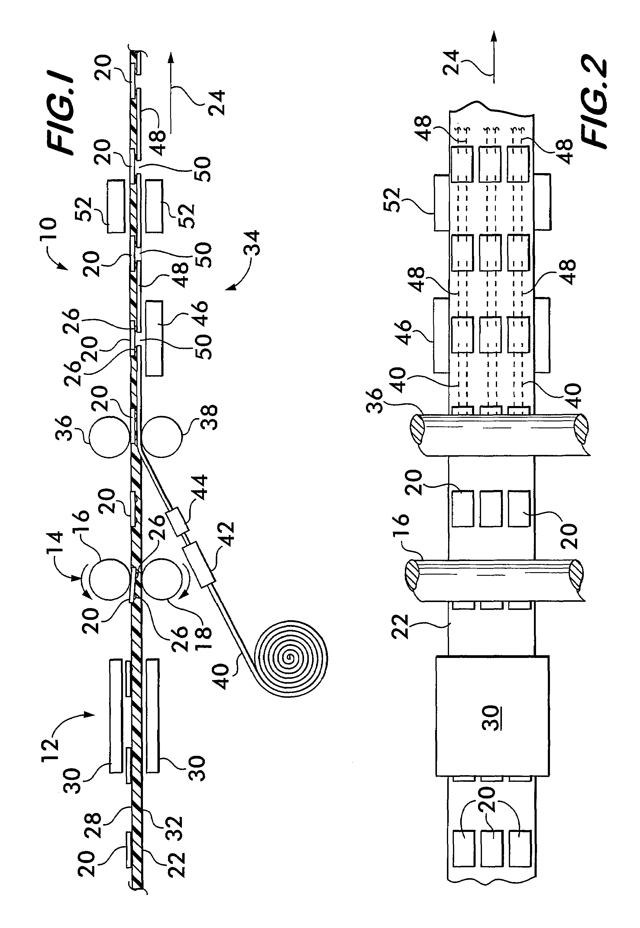
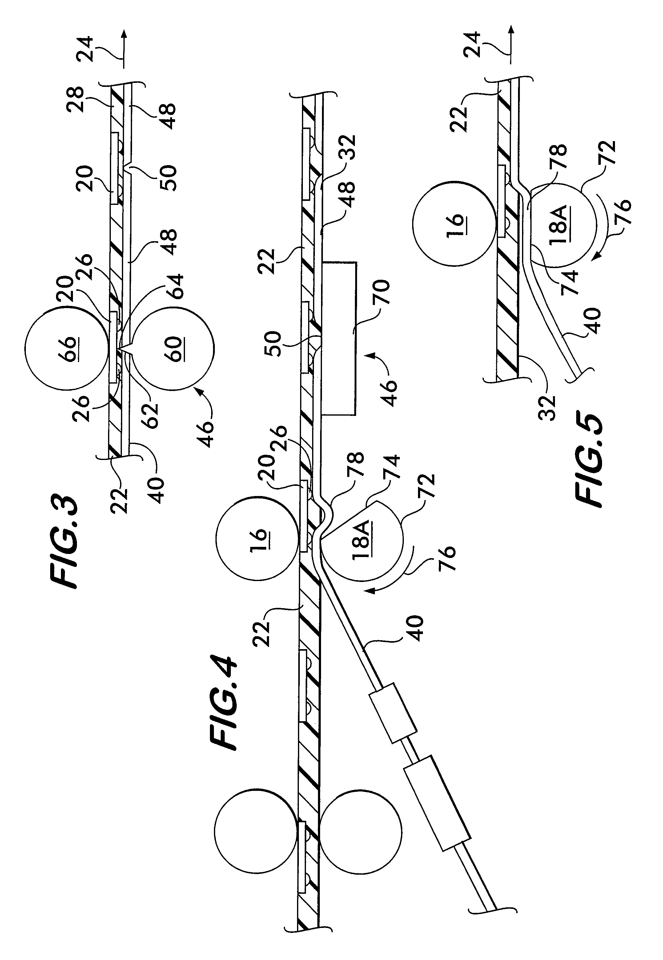
[0052]An exemplary embodiment for an in-mold chip strap and approach for making an in-mold strip is shown in FIGS. 1 and 2. As can best be seen in the side sectional view of FIG. 1, a manufacturing device 10 for making an embedded chip strap includes a heater 12 and a rotary station 14 having two rollers 16 and 18 that embeds chips 20 into a layer of poly (e.g., polymer, polyester, polyurethane, polystyrene, PVC), also referred to as a poly sheet 22, moving continuously in a machine direction 24. The poly sheet 22 includes a first layer or side (e.g., top side 28) and a second layer or side (e.g., bottom side 32) opposite the first layer or side. In this embodiment, the chips 20 are placed onto the poly sheet 22 before the poly sheet is heated by the heater 12 to just below its glass thermal temperature. However, the scope of the invention is not limited to this order, as the poly sheet 22 could also be heated to just below its glass thermal temperature before or while the chips 20 ...


PUM

PropertyMeasurementUnit
sizeaaaaaaaaaa
depthaaaaaaaaaa
depthaaaaaaaaaa

Abstract

A poly sheet continuously moving in a machine direction is heated to a temperature just below its glass thermal temperature to make the poly malleable. A circuit (e.g., RFID chip, EAS chip, transponder, IC) is placed on the poly sheet and embedded into the poly sheet, preferably with a heat resistant soft (e.g., rubber) roller that presses the circuit into the poly without breaking the circuit. A conductive strip or wire may be applied on or into the poly sheet to align with connection points (e.g., conductive bumps) of the circuit for conductive communication with the circuit. The conductive strip or wire is preferably cut to form gaps that are nonconductive between the cut sections of wire to avoid shorting of the circuit and / or allow the conductive strip or wire to function as an antenna for the circuit, and thus to form a chip strap or tag. The poly sheet thus provides a protective womb or shield for the circuit and wire.

Description

CROSS-REFERENCE TO RELATED APPLICATIONS[0001]This utility application claims the benefit under 35 U.S.C. §119(e) of Provisional Application Ser. No. 60 / 732,898 filed on Nov. 2, 2005 and Provisional Application Ser. No. 60 / 744,461 filed Apr. 7, 2006, both entitled IN-MOLD CHIP ATTACH and whose entire disclosures are incorporated by reference herein.BACKGROUND OF THE INVENTION[0002]1. Field of Invention[0003]This invention is related to communication devices, and in particular, to the manufacture of security tags often use, for example, as Radio Frequency Identification (RFID) circuits.[0004]2. Description of Related Art[0005]Chip bonding is costly. The two largest components of the cost of RFID tags today are the integrated circuit and the attachment of that circuit (otherwise known as silicon) to an antenna structure. While the increasing volume of the number of chips helps to drive the IC cost down, bonding is a mechanical process and does not benefit from the same technology advan...

Claims


Application Information

Patent Timeline
Patent Type & Authority Patents(United States)
IPC IPC(8): H05K3/07
CPCG06K19/07749G06K19/0775G08B13/244H01L21/56H01L21/67132H01L24/86H01L24/96H01L24/97G06K19/07718H01L2924/3025Y10T29/49155H01L2224/16H01L2224/7965H01L2924/01013H01L2924/01015H01L2924/01029H01L2924/01033H01L2924/01079H01L2924/01082H01L2924/14H01L2924/30105H01L2924/01006H01L2924/01074H01L2924/014Y10T428/14Y10T29/4916Y10T29/49158H01L2924/181H01L2924/12042H01L2924/00
Inventor COTE, ANDREDUSCHEK, DETLEF
Owner CHECKPOINT SYST INC
Features
  • R&D
  • Intellectual Property
  • Life Sciences
  • Materials
  • Tech Scout
  • Unparalleled Data Quality
  • Higher Quality Content
  • 60% Fewer Hallucinations
Learn More