Method of manufacturing semiconductor device and liquid immersion lithography system

a technology of liquid immersion lithography and semiconductor devices, which is applied in the direction of photomechanical treatment, printing, instruments, etc., can solve the problem of film being peeled

Inactive Publication Date: 2009-12-08
KK TOSHIBA
View PDF11 Cites 13 Cited by
  • Summary
  • Abstract
  • Description
  • Claims
  • Application Information

AI Technical Summary

Problems solved by technology

When the adhesiveness between the film formed on the wafer and the wafer is insufficient, the film may be peeled when the liquid immersion fluid passes through the edge of the wafer.
Even though the peeled films are not curled like particles and kept in the shapes of flakes, the peeled films may serve as origin of a pattern defect in any case because refraction indexes of the films and the liquid immersion fluid are different from each other and because the films cannot be kept perpendicular to a plurality of refracted lights.
However, Document 2 does not describe timing at which tool cleaning is performed and a trigger for the cleaning at all.

Method used


Image

  • Method of manufacturing semiconductor device and liquid immersion lithography system
  • Method of manufacturing semiconductor device and liquid immersion lithography system
  • Method of manufacturing semiconductor device and liquid immersion lithography system

Examples


first embodiment

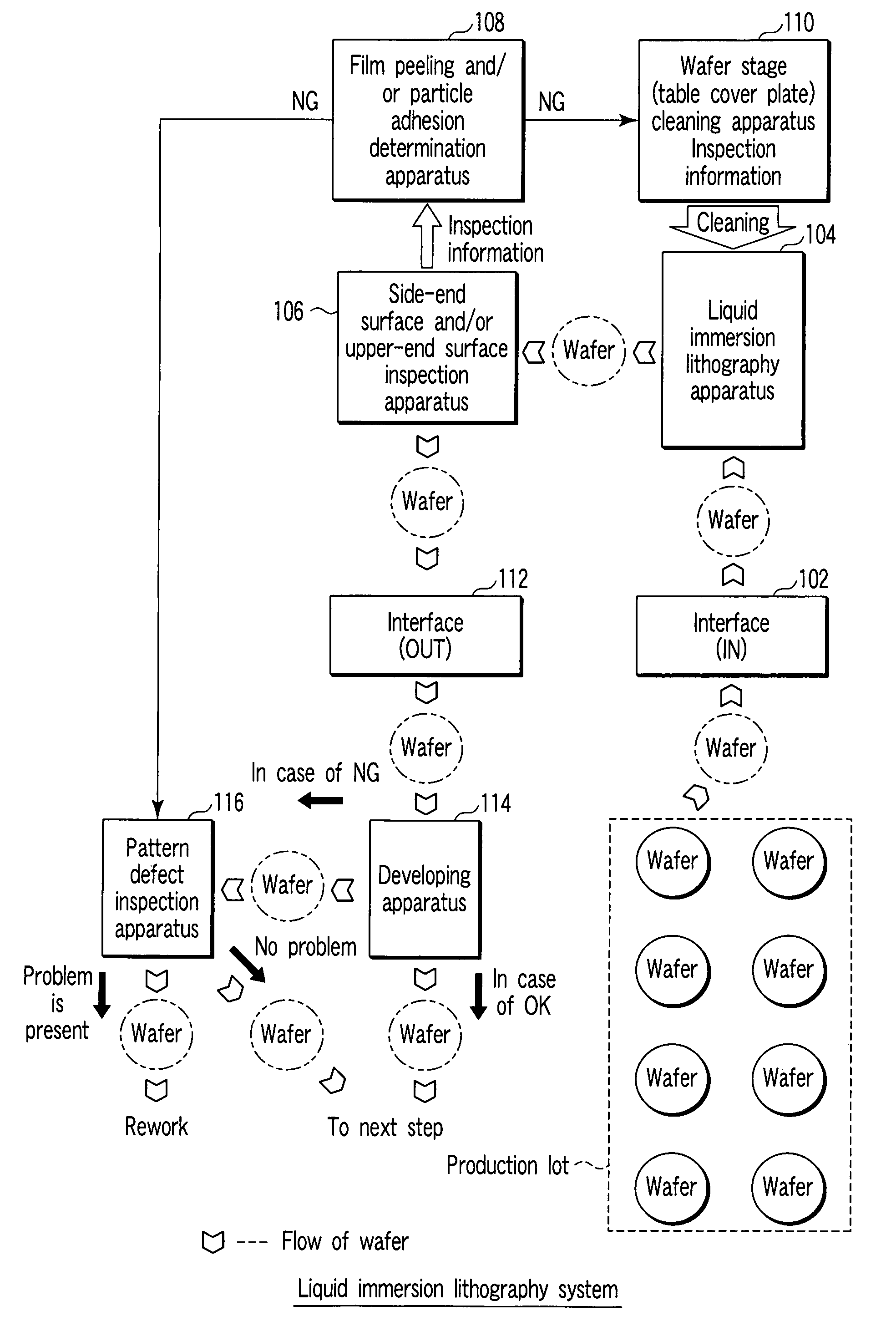
[0073]An outline of a lithography system including an inspection step for adhesion of particles generated by film peeling on an edge face of a wafer by relative movement of liquid immersion fluid or film peeling caused by a wafer exposed in advance in the liquid immersion lithography apparatus described in Reference 1 and 2, and a coping process performed when the film peeling occurs will be described below.

[0074]A flow chart of the embodiment is shown in FIG. 9. A “coating” step in the flow chart includes all the processes performed until a wafer is given to the liquid immersion lithography apparatus in the coating and developing apparatus. A “developing” step includes all processes in the coating and developing apparatus after the pattern exposure step performed by the liquid immersion lithography apparatus.

[0075]After the pattern exposure process performed by the liquid immersion lithography apparatus, predetermined inspection is performed to detect film peeling, and adhesive mat...

second embodiment

[0093]As a method of inspecting an wafer edge, a detecting mechanism which is the same as the wafer edge face inspection apparatus or a detecting mechanism incorporated in a bevel polishing apparatus can be used. More specifically, the method is constituted by: a detecting mechanism constituted by an optical system including a lens, an optical filter as needed, and an image detecting unit such as a CCD, a storing device, and an image processing device; and a mechanism which moves either one of or both of a wafer edge used to inspect an interested position on the outer periphery of the wafer, and the detecting mechanism.

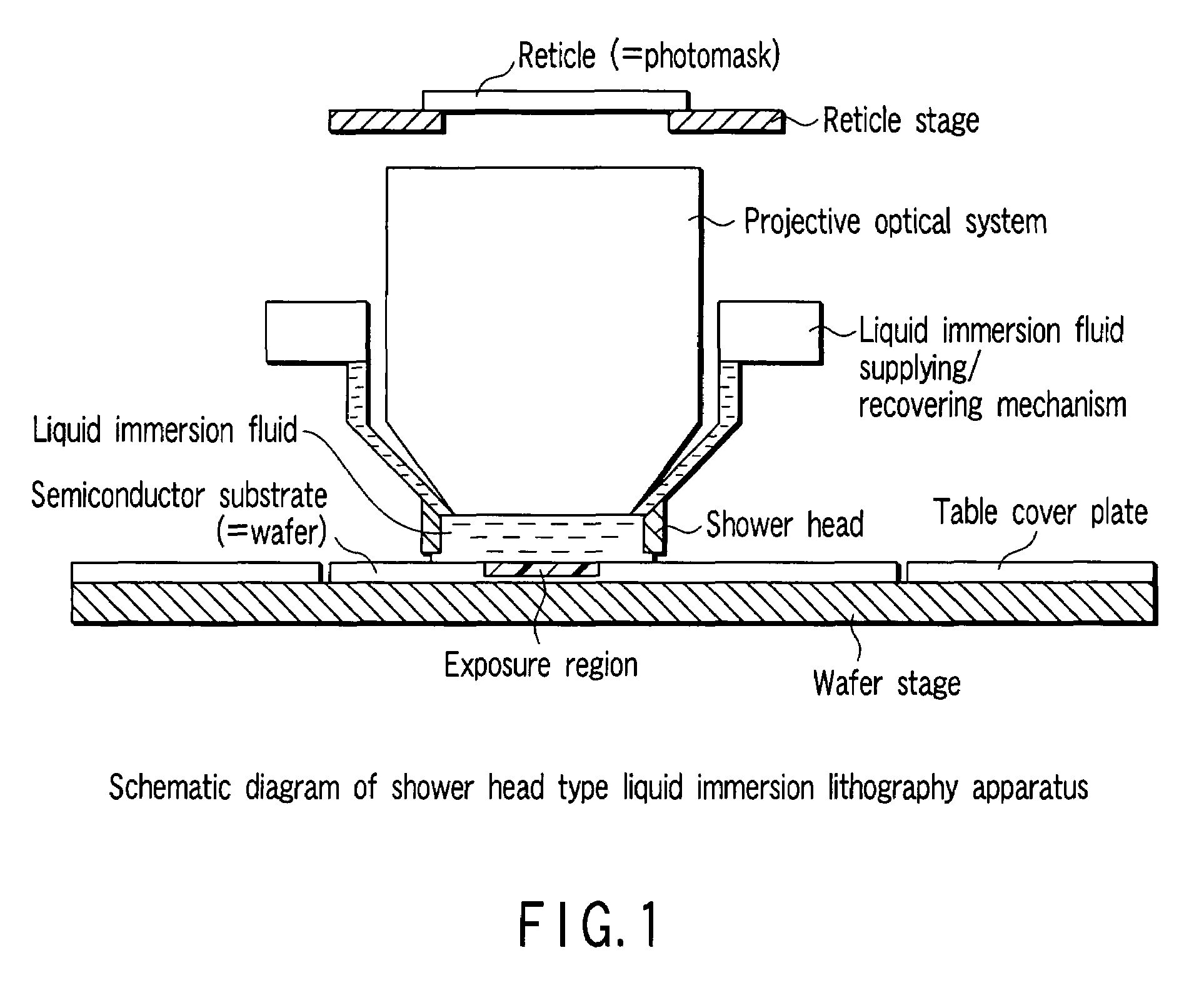
[0094]By relative movement between liquid immersion fluid and a wafer in liquid immersion lithography, on an upper surface side of the wafer which may be in contact with the liquid immersion fluid and on a side surface of the wafer on which a flow of liquid immersion fluid is supposed to be disturbed to some extent, film peeling at an edge of the wafer may occur.

[0095...

third embodiment

[0099]An example obtained by improving the method of inspecting a wafer edge in the second embodiment will be described below.

[0100]In the second embodiment, in order to detect film peeling or adhesion of particles at an edge of a wafer, before and after the pattern exposure step performed by the liquid immersion lithography apparatus, the edge of the wafer is inspected, and the film peeling or the adhesion of particles is detected on the basis of both pieces of inspection information.

[0101]As described in the second embodiment, when detection is performed only after the liquid immersion pattern exposure step, ununiformity of a film composition which is present at the edge of the wafer before the liquid immersion pattern exposure step without causing film peeling in the liquid immersion pattern exposure step or adhesion of particle may be detected. In order to prevent such false detection, a method of inspecting the edge of the wafer before and after the liquid immersion pattern exp...


PUM


Abstract

A method of manufacturing a semiconductor device is disclosed. The manufacturing method includes the following steps in a period from a liquid immersion lithography step to a step in which a film structure of at least an edge of a wafer changes from a timing of the liquid immersion lithography step. At least one of a side surface of an edge of the wafer and an upper surface of the edge of the wafer is inspected. On the basis of an inspection result, at least one of the presence / absence of film peeling and the presence / absence of particle adhesion is determined on at least one of the side surface of the edge of the wafer and the upper surface of the edge of the wafer. A predetermined coping process is performed when it is determined that at least one of the film peeling and the particle adhesion has occurred.

Description

CROSS-REFERENCE TO RELATED APPLICATIONS[0001]This application is based upon and claims the benefit of priority from prior Japanese Patent Application No. 2006-085664, filed Mar. 27, 2006, the entire contents of which are incorporated herein by reference.BACKGROUND OF THE INVENTION[0002]1. Field of the Invention[0003]The present invention relates to a method of manufacturing a semiconductor device and, in particular, to a method of manufacturing a semiconductor device using liquid immersion lithography and a liquid immersion lithography system.[0004]2. Description of the Related Art[0005]As a next-generation lithography technique for 193 nm lithography, the development of 193 nm liquid immersion lithography has been advanced. A schematic diagram of a liquid immersion lithography apparatus is shown in FIG. 1.[0006]As shown in FIG. 1, in liquid immersion lithography, a part between a last element of an objective lens of the lithography apparatus and a semiconductor substrate (wafer) on...

Claims


Application Information

Patent Timeline
Patent Type & Authority Patents(United States)
IPC IPC(8): G03B27/52G03B27/42
CPCG03F7/70341G03F7/70916G03F7/70866G03F7/2014
Inventor KAWAMURA, DAISUKE
Owner KK TOSHIBA
Why Eureka
Try Eureka