Semiconductor device and its manufacturing method
a semiconductor device and manufacturing method technology, applied in the field of semiconductor devices, can solve the problems of increasing the manufacturing cost of image pickup devices, and achieve the effects of enhancing the reliability of semiconductor devices, preventing short circuit trouble, and high precision
- Summary
- Abstract
- Description
- Claims
- Application Information
AI Technical Summary
Benefits of technology
Problems solved by technology
Method used
Image

Examples
first embodiment
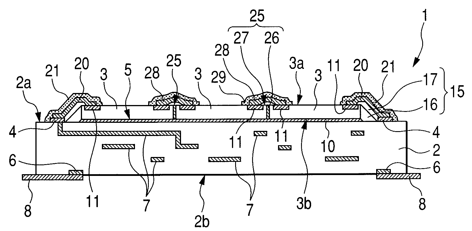
[0161]FIGS. 1 through 21 are diagrams relating to a semiconductor device and its manufacturing method in accordance with a first embodiment of the present invention. FIGS. 1 through 6 are diagrams relating to the semiconductor device and FIGS. 7 through 21 are diagrams relating to the semiconductor device manufacturing method.
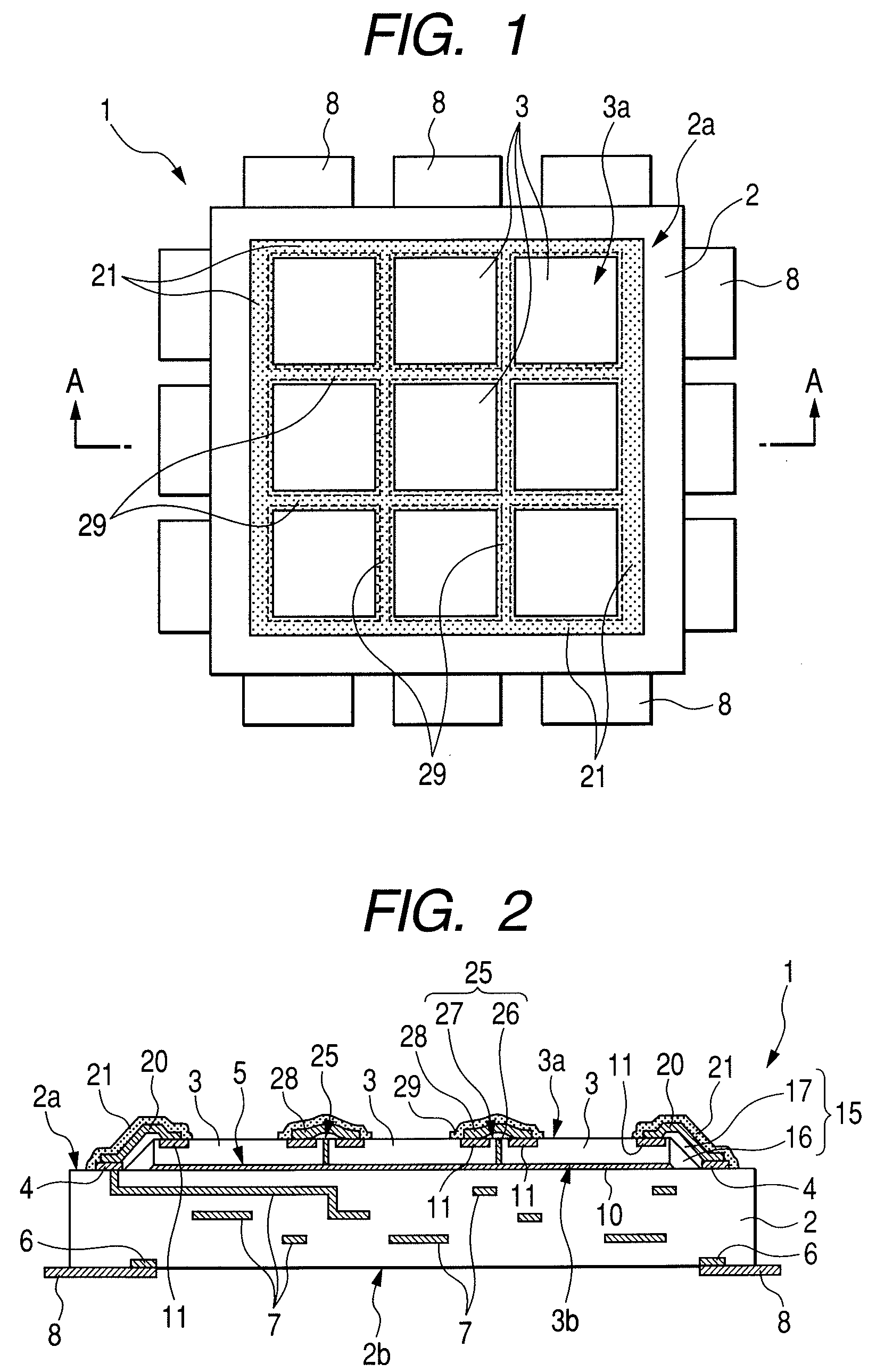
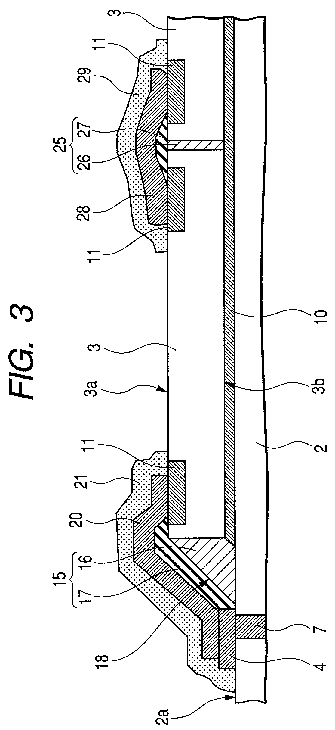
[0162]In the first embodiment, the semiconductor device in which semiconductor chips as electronic parts are arrayed lengthwise and crosswise on a wiring substrate, as shown in FIG. 1 and FIG. 2, is described. A semiconductor chip is a sensor chip that receives light and converts it into electrical signals. Accordingly, the semiconductor device makes an image pickup device. FIG. 1 is a schematic plan view of the semiconductor device. FIG. 2 is a schematic sectional view taken along an A-A line in FIG. 1. FIG. 3 is an enlarged sectional view of a part of FIG. 2. FIG. 4 is an enlarged sectional view of a part of FIG. 3. FIG. 5 is an enlarged sectional view showin...
second embodiment
[0226]A second embodiment presents an example of arraying and fixing plural semiconductor chips in the first embodiment onto a wiring substrate (chip tiling). FIGS. 22 through 24 relate to diagrams showing an example of arraying and fixing semiconductor chips onto a wiring substrate (chip tiling). By the chip timing, the multiple chips are arrayed in a matrix without clearance between chips.
[0227]As shown in FIG. 22A, a flat basin 35 holding a liquid (solution) 36 is prepared and plural semiconductor chips are allowed to float in the liquid 36. Preferably, the liquid has a large surface tension; for example, an agar solution is used. The semiconductor chips 3 are sensor chips and floated in the liquid 36 with the first surface 3a having the image pickup surface facing down. The semiconductor chips gather together 3 as shown in FIG. 24A by the force of the liquid 36 agitated by placing the chips on the surface of the liquid 36 and the surface tension of the liquid 36. However, at thi...
third embodiment
[0249]FIG. 27 and FIG. 28 relate to a semiconductor device in accordance with a third embodiment of the present invention. FIG. 27 is a schematic plan view of the semiconductor device and FIG. 28 is a schematic enlarged sectional view taken along a J-J line in FIG. 27.
[0250]The third embodiment is a semiconductor device 1A formed by chip tiling of a cluster of chips on a removable adhesive tape. In the process for the semiconductor device 1A of the third embodiment, after the semiconductor chips 3 are aligned in close contact with each other in a matrix on the surface of the liquid 36, as described in the second embodiment and shown in FIG. 24B, the liquid 36 is left as is to turn to the hardening body 37. Instead of fixing the semiconductor chips 3 to the wiring substrate 2 via the bonding material 10, as shown in FIG. 23A, then, an adhesive tape 42 having the adhesive surface (adhesive layer 43) is put on the second surface 3b of the semiconductor chips 3, thus sticking the semico...
PUM
 Abstract
Description
Claims
Application Information
 - R&D Engineer
- R&D Manager
- IP Professional
- Industry Leading Data Capabilities
- Powerful AI technology
- Patent DNA Extraction
Browse by: Latest US Patents, China's latest patents, Technical Efficacy Thesaurus, Application Domain, Technology Topic.
© 2024 PatSnap. All rights reserved.Legal|Privacy policy|Modern Slavery Act Transparency Statement|Sitemap