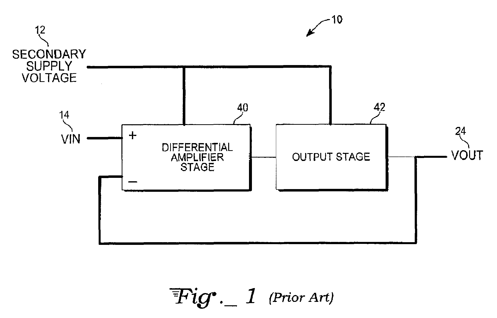
Unity gain voltage buffer with dual supply voltage for managing current consumption in low voltage applications
a dual supply voltage and gain voltage technology, applied in pulse manipulation, instruments, pulse techniques, etc., can solve the problems of large charge pump, disadvantageous current load on vpp, and limited output current,
- Summary
- Abstract
- Description
- Claims
- Application Information
AI Technical Summary
Problems solved by technology
Method used
Image

Examples
Embodiment Construction
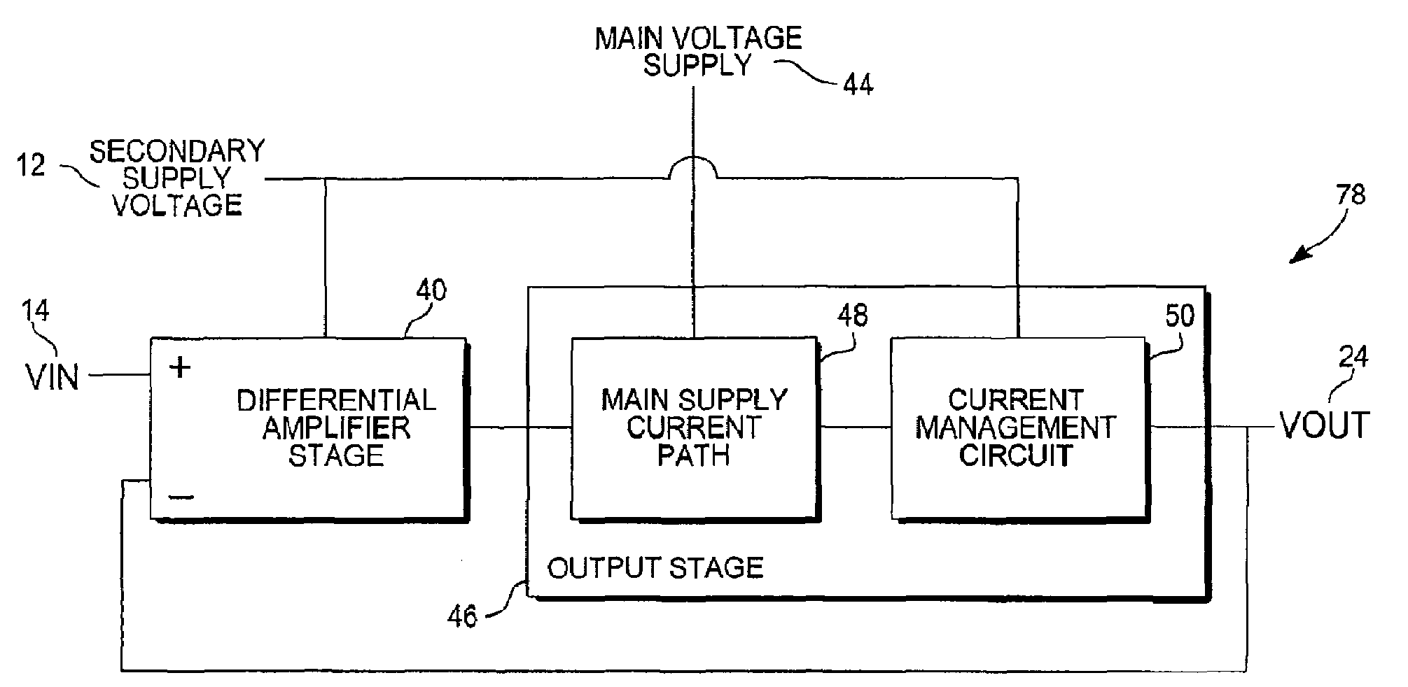
[0015]An exemplary embodiment of a unity gain voltage buffer circuit 78 is shown in FIG. 3. The input voltage 14 and feedback output voltage 24 are compared at differential amplifier stage 40. The difference between the voltages drives the output stage 46, which includes a main supply current path 48, supplied by the main voltage supply 44 and a current management circuit 50 and is supplied by the secondary supply voltage 12. The output voltage 24 replicating the input voltage 14 is provided by both the main voltage supply 44 and, as discussed in greater detail below, the secondary voltage supply 12. The output voltage 24 has a higher current output capability than the input voltage 14.
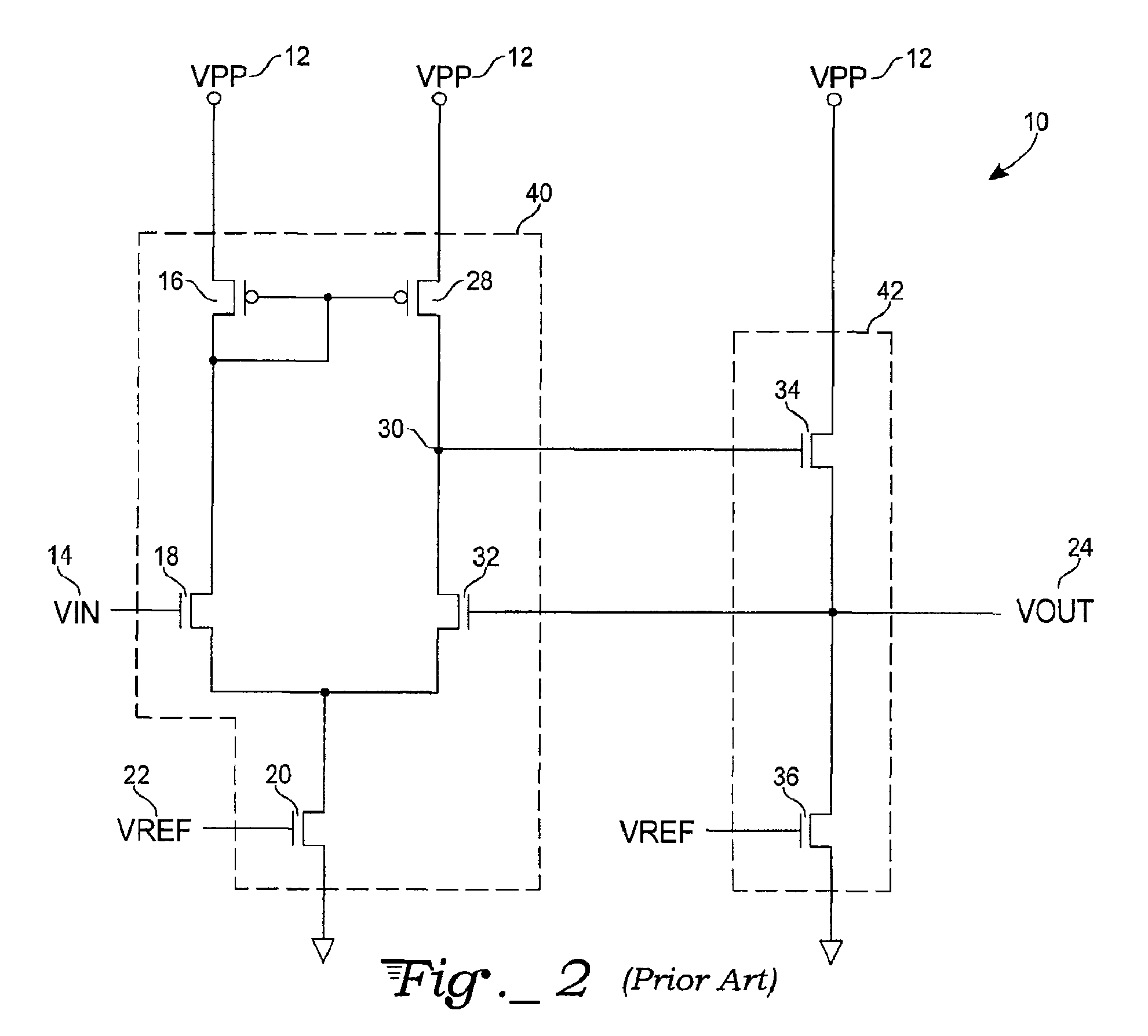
[0016]A circuit diagram of an exemplary embodiment of a unity gain voltage buffer circuit 78 is shown in FIG. 4. The differential amplifier stage 40 is supplied by secondary or auxiliary supply voltage VPP 12. Transistors 16, 18, 20, 28, and 32 form a differential amplifier stage which is well known t...
PUM
 Abstract
Description
Claims
Application Information