Apparatus and method for interfacing to a memory

a technology of memory and apparatus, applied in the field of apparatus and a memory interface, can solve the problems of complex implementation, large challenge of interfacing to external memory at high clock rate, and standard design techniques that are not proven to provide a feasible solution to interfacing with external memory at these data ra

Active Publication Date: 2010-02-09
MOSAID TECH
View PDF14 Cites 27 Cited by
  • Summary
  • Abstract
  • Description
  • Claims
  • Application Information

AI Technical Summary

Problems solved by technology

One area of issue is the external memory interface, which is an intermediary device between the system, such as a processor, and a memory, such as static random access memory (SRAM).
However, interfacing to external memory at high clock rates poses a large challenge due to the reduced clock cycle and various system timing skews, such as voltage and temperature variation, crosstalk, Vref variations, simultaneous-switching output (SSO) noise and simultaneous-switching input (SSI) noise, and clock source jitter.
After applying the various system timing offsets to these allowances, standard design techniques are proven to not provide a feasible solution to interfacing with these memories at these data rates.
Custom techniques may provide a solution, however these solutions are complex to implement, do not fit into ASIC design flows, are not readily re-usable, and require large efforts to port between foundries or process nodes.
The disadvantage of this approach is the inability to meet high data rates.
As an example, solutions such as these typically achieve approximately 166 MHz, but fail to operate properly between 200 MHz-250 MHz, even after a high degree of manual intervention, which is not easy to implement.
Therefore, desired high performance clock rates, such as 333 MHz cannot be easily achieved.
There are three primary issues that must be considered for a synthesized QDR2 SRAM memory interface design.
This is difficult to achieve with a synthesizeable solution due to the pseudo-random nature of synthesis and optimization tools, and of placement and routing tools.
In otherwords, circuit element layout and signal line routing cannot be precisely controlled.
Clock generation can be a particularly difficult issue.
The PVT (Process / Voltage / Temperature) sensitive nature of standard cell elements causes these clock / data relationships to be unreliable at high data rates.
This requires a wide distribution of 2× frequency clocks, which complicates chip implementation and verification.
Some synthesized solutions rely on the falling edge of the system clock, which introduces duty cycle problems into the design, further reducing the achievable data rate.
Secondary tools within the ASIC flows for tasks such as DFT (design for test) and boundary scan insertion, tend to add to the problems of pseudo-random gates, placements, and routing.
Hence, the pseudo-random nature of the resultant interface adds tremendous overhead to product test and debug tasks since every pin of the interface has the potential for a differing response to PVT variations, electrical noise, and source clock uncertainties.
However, several issues still remain, as is described below.
Accordingly, implementation complexity remains high.

Method used


Image

  • Apparatus and method for interfacing to a memory
  • Apparatus and method for interfacing to a memory
  • Apparatus and method for interfacing to a memory

Examples


Embodiment Construction

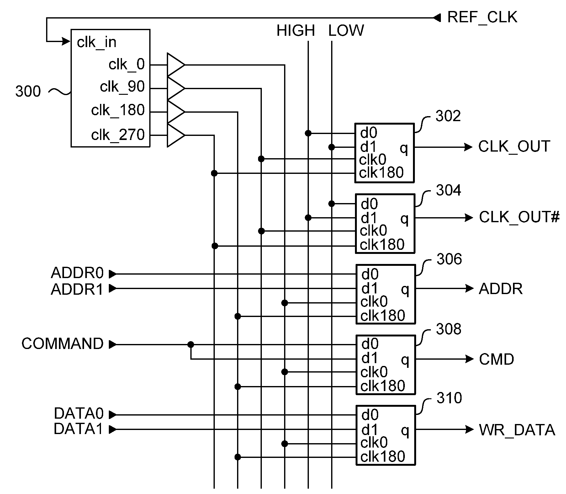
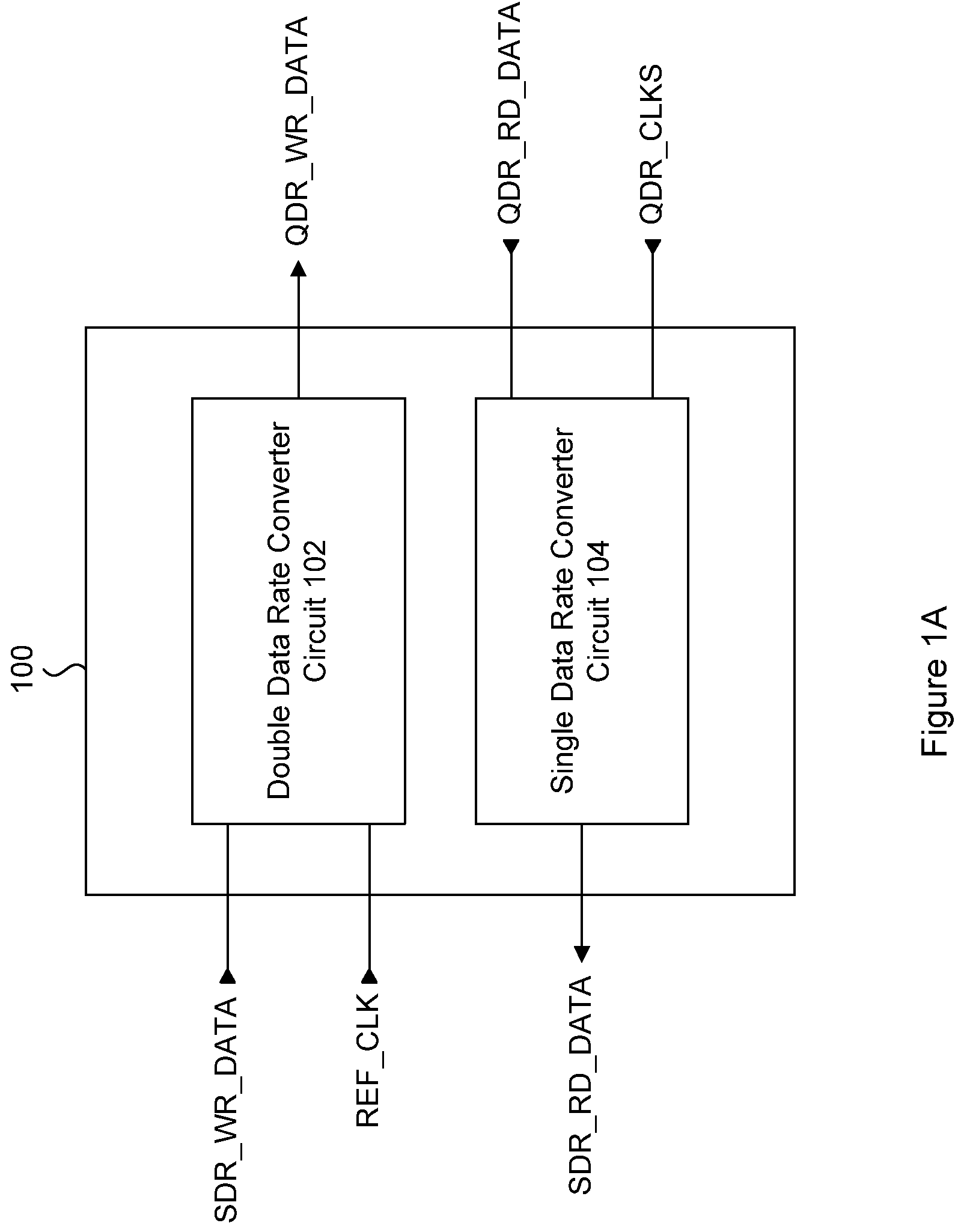
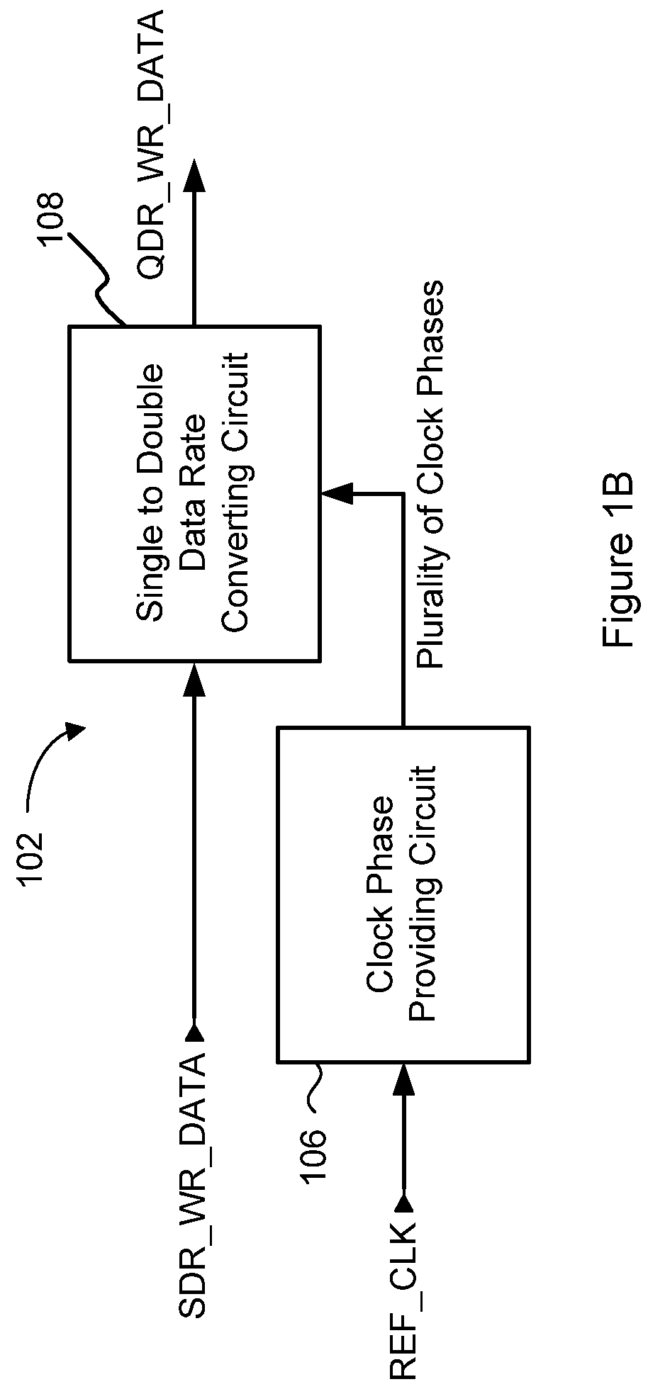
[0043]A delay locked loop (DLL) is added to the system in order to provide an accurate, PVT insensitive translation of the drive clocks into the write data eye. Adding a master-slave DLL to the system provides an accurate, PVT insensitive translation of the echo clocks into the read data eye. Solidifying the timing critical drive and receive logic which directly interfaces to the I / O buffers reduces the pin-to-pin skews. Utilizing clock phase outputs of the DLL in the solidified drive and receive logic blocks reduces further the skew between the clock and related data signals, and also removes the reliance on a differential clock. The system allows a much more relaxed constraint on clock duty cycle. Design of circuitry within the solidified drive and receive logic blocks permits simple logic modeling for fit within an ASIC flow. Physical design of the solidified drive and receive logic blocks permits simple fit within ASIC place and route flows for increased ease of implementation a...


PUM


Abstract

A delay locked loop (DLL) is added to the system in order to provide an accurate, PVT insensitive translation of the drive clocks into the write data eye. Adding a master-slave DLL to the system provides an accurate, PVT insensitive translation of the echo clocks into the read data eye. Solidifying the timing critical drive and receive logic which directly interfaces to the I / O buffers reduces the pin-to-pin skews. Utilizing clock phase outputs of the DLL in the solidified drive and receive logic blocks reduces further the skew between the clock and related data signals, and also removes the reliance on a differential clock. The system allows a much more relaxed constraint on clock duty cycle. Design of circuitry within the solidified drive and receive logic blocks permits simple logic modeling for fit within an ASIC flow. Physical design of the solidified drive and receive logic blocks permits simple fit within ASIC place and route flows for increased ease of implementation and ease of reuse.

Description

REFERENCE TO RELATED APPLICATIONS[0001]This application claims the benefit of priority of U.S. Provisional Patent Application No. 60 / 803,557 entitled “Apparatus and Method for Interfacing to a Memory” filed May 31, 2006, the contents of which are entirely incorporated herein by reference.FIELD OF THE INVENTION[0002]The present invention relates generally to memory interface architecture. More particularly, the present invention relates to an apparatus and a method for interfacing to a memory.BACKGROUND OF THE INVENTION[0003]Presently, high performance systems rely on advanced technology, higher processor clock rates and higher data rates to and from these processors. One area of issue is the external memory interface, which is an intermediary device between the system, such as a processor, and a memory, such as static random access memory (SRAM). There are different types of SRAM available, each type adhering to a particular set of operating protocols. For example, there is double d...

Claims


Application Information

Patent Timeline
Patent Type & Authority Patents(United States)
IPC IPC(8): G06F1/00
CPCG11C7/1012G11C7/1066G11C7/22G11C7/222G11C11/41G11C2029/5602
Inventor DEFAZIO, JODYBECCA, OSWALDNYASULU, PETER
Owner MOSAID TECH
Why Eureka
Try Eureka