Dual side cooling integrated power device package and module with a clip attached to a leadframe in the package and the module and methods of manufacture

a technology of integrated power devices and leadframes, which is applied in the direction of semiconductor devices, semiconductor/solid-state device details, electrical apparatus, etc., can solve the problem that the heat dissipation capacity of leads only is not sufficient to provide reliable operation of power devices, and the amount of space required for wire bonds in conventional packages is not enough

Active Publication Date: 2010-02-16
SEMICON COMPONENTS IND LLC
View PDF13 Cites 37 Cited by
  • Summary
  • Abstract
  • Description
  • Claims
  • Application Information

AI Technical Summary

Problems solved by technology

However, such small packages provide problems in terms of dissipating heat from packaged power devices used in the electronic circuits.
In many cases the heat dissipating capacity of the leads only is not sufficient to provide reliable operation of the power device.
Another factor in forming compact circuits is the amount of space required for wire bonds in conventional packages.
Although the integrated transistor module of the latter published patent publication is useful for the applications for which it was intended, the module footprint is not a common one in the industry.

Method used


Image

  • Dual side cooling integrated power device package and module with a clip attached to a leadframe in the package and the module and methods of manufacture
  • Dual side cooling integrated power device package and module with a clip attached to a leadframe in the package and the module and methods of manufacture
  • Dual side cooling integrated power device package and module with a clip attached to a leadframe in the package and the module and methods of manufacture

Examples


Embodiment Construction

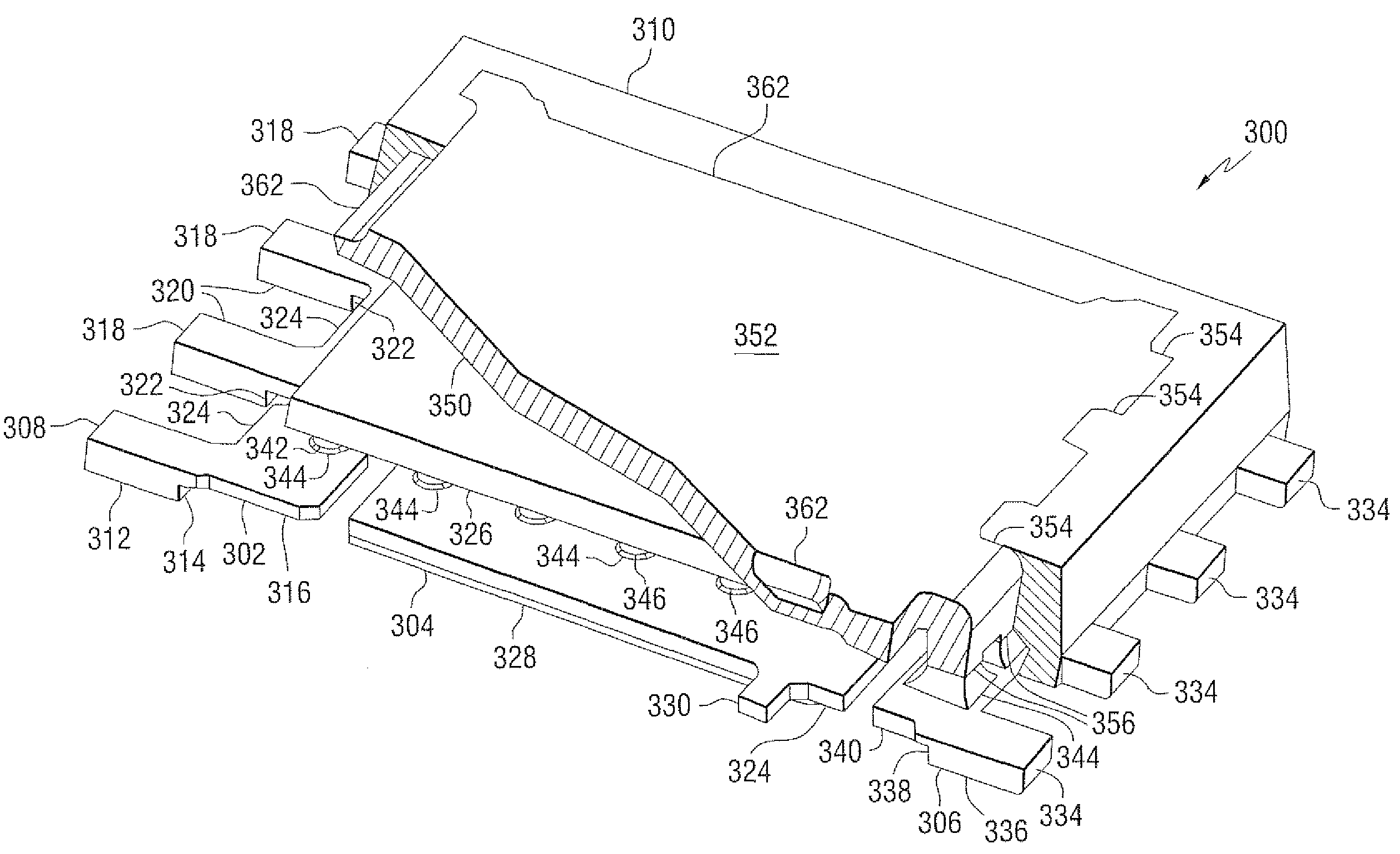
[0055]Embodiments of the invention are directed to semiconductor die packages and methods for making semiconductor die packages. A semiconductor die package according to an embodiment of the invention includes a substrate, and a semiconductor die mounted on the substrate. The semiconductor die may at attached to the substrate using an adhesive or any other suitable attachment material. In the semiconductor die package, the bottom surface and / or the top surface of the semiconductor die may be electrically coupled to conductive regions of the substrate. An encapsulating material may encapsulate the semiconductor die. As will be explained in further detail below, the substrates according to embodiments of the invention can have different configurations in different embodiments.

[0056]The substrate may have any suitable configuration. However, in preferred embodiments of the invention, the substrate includes a leadframe structure and a molding material. Typically, at least one surface of...


PUM


Abstract

An integrated power device module having a leadframe structure with first and second spaced pads and one or more common source-drain leads located between said first and second pads, first and second transistors flip chip attached respectively to said first and second pads, wherein the source of said second transistor is electrically connected to said one or more common source-drain leads, and a first clip attached to the drain of said first transistor and electrically connected to said one or more common source-drain leads. In another embodiment a partially encapsulated power quad flat no-lead package having an exposed top thermal drain clip which is substantially perpendicular to said with a folded stud exposed top thermal drain clip, and an exposed thermal source pad.

Description

CROSS-REFERENCE TO RELATED APPLICATIONS[0001]This application is a continuation-in-part of U.S. patent application Ser. No. 11 / 740,475 which claims the benefit of U.S. Provisional Patent Application Ser. No. 60 / 802,181, filed on May 19, 2006, which application is hereby incorporated by reference. This application also claims the benefit of U.S. Provisional Application Ser. No. 60 / 916,994, filed on May 9, 2007, which application is hereby incorporated by reference. Reference is also made to a related application Ser. No. 11 / 625,100, filed Jan. 19, 2007 entitled “Flip Chip MLP with Folded Heat Sink” which is also incorporated herein by reference.FIELD OF THE INVENTION[0002]This invention relates in general to packaging of semiconductor devices and more particularly to a dual side cooling integrated power device module and methods of making same.BACKGROUND OF THE INVENTION[0003]Small packages for semiconductors with short leads are desirable for forming electronic circuits which are co...

Claims


Application Information

Patent Timeline
Patent Type & Authority Patents(United States)
IPC IPC(8): H01L23/495H01L21/60H01L23/02H01L23/48
CPCH01L23/3107H01L23/36H01L23/49524H01L23/49548H01L23/49562H01L23/49575H01L24/36H01L24/40H01L2924/1305H01L2924/1306H01L2224/37147H01L2224/73253H01L2224/32245H01L2924/014H01L2924/01047H01L2924/01024H01L2924/01006H01L2924/01005H01L2224/32057H01L2224/49171H01L2224/73255H01L2224/83385H01L2924/01013H01L2924/01015H01L2924/01027H01L2924/01029H01L2924/01033H01L2924/01046H01L2924/01078H01L2924/01079H01L2924/01082H01L2924/13091H01L2924/14H01L2924/30107H01L24/48H01L24/49H01L2224/16245H01L2224/48247H01L2924/00H01L24/37H01L2224/05554H01L2224/40245H01L2224/40095H01L2924/181H01L2924/00012H01L2924/00014H01L2224/84801H01L2224/83801H01L24/84H01L2224/45099H01L2224/45015H01L2924/207H01L2224/73221H01L23/42
Inventor NOQUIL, JONATHAN A.MADRID, RUBEN
Owner SEMICON COMPONENTS IND LLC
Why Eureka
Try Eureka