Phase change memory device

a memory device and phase change technology, applied in the field of phase change memory devices, can solve the problems of deterioration in the data sensing margin and yield of the chip, degraded low sensing efficiency of the phase change memory device, so as to improve the sensing efficiency of the sense amplifier, improve the stability and accuracy of the clamp voltage, and improve the stability and accuracy of the reference current.

Active Publication Date: 2010-02-16
SK HYNIX INC
View PDF6 Cites 11 Cited by
  • Summary
  • Abstract
  • Description
  • Claims
  • Application Information

AI Technical Summary

Benefits of technology

[0016]Embodiments of the present invention include a phase change memory device having phase change resistors that provides improved stability and accuracy of reference currents using a reference cell array that is under the same conditions as a cell array.
[0017]Additionally, embodiments of the present invention include a phase change memory device having phase change resistors that provides improved stability and accuracy of clamp voltages using a clamp cell array that is under the same conditions as a cell array.
[0018]Additionally, embodiments of the present invention include a phase change memory device having phase change resistors that improves the sensing efficiency of a sense amplifier using a reference cell array having the same timing delay element.
[0019]Additionally, embodiments of the present invention include a phase change memory device having phase change resistors that improves the offset characteristic of a sense amplifier.

Problems solved by technology

However, phase change memory devices are not without problems.
When the reference voltage of a phase change memory device having phase change resistors is not effectively controlled, the sensing efficiency of a sense amplifier is degraded.
As such, the reference current is unstable, and the accuracy and the offset characteristic of the sense amplifier are degraded causing deterioration in the data sensing margin and yield of a chip.

Method used


Image

  • Phase change memory device
  • Phase change memory device
  • Phase change memory device

Examples


Embodiment Construction

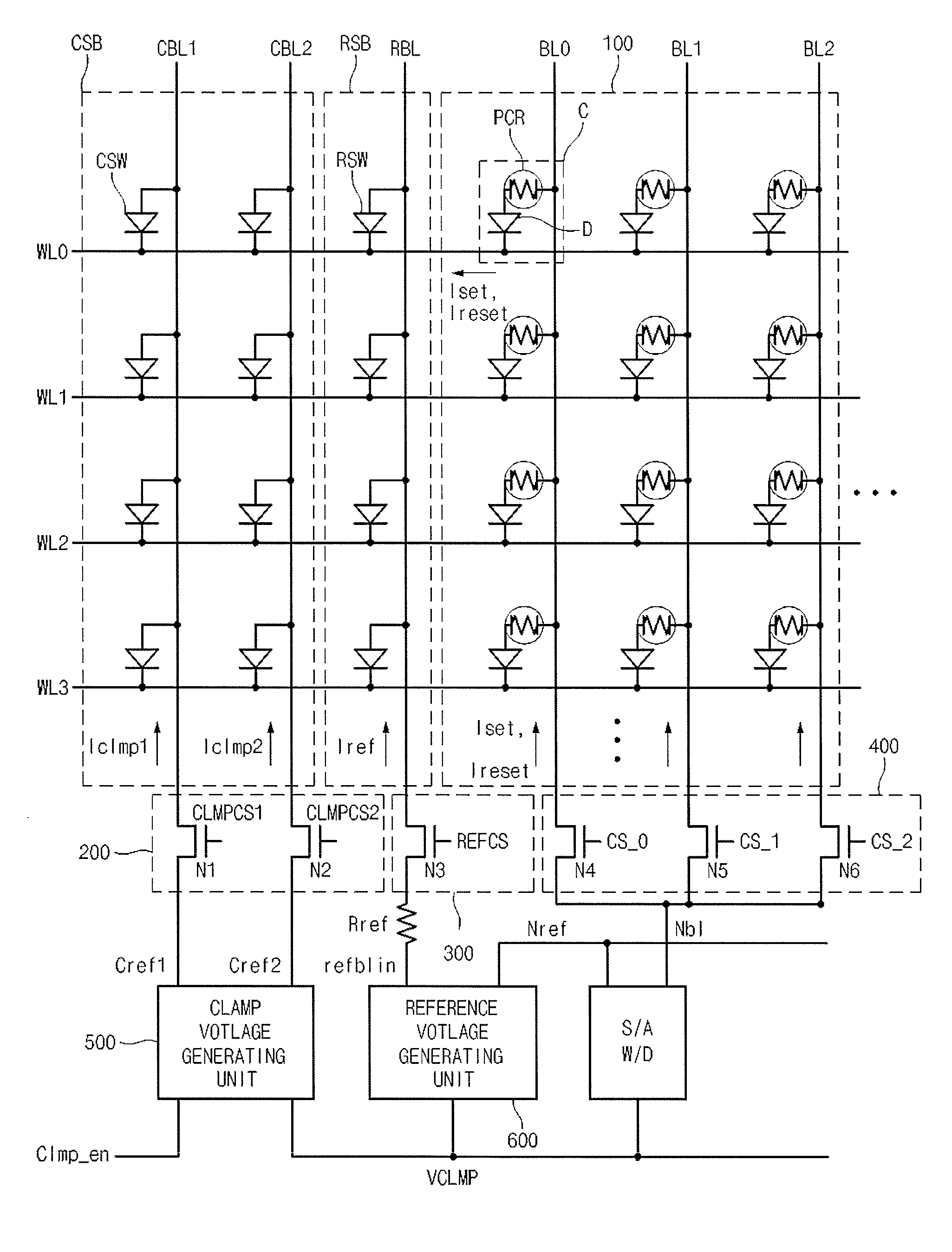
[0041]FIG. 4 is a circuit diagram showing a phase change memory device according to an embodiment of the present invention.

[0042]The phase change memory device shown in FIG. 4 comprises a clamp cell array block CSB, a reference cell array block RSB, a cell array block 100, a clamp column selecting unit 200, a reference column selecting unit 300, a column selecting unit 400, a reference resistor Rref, a clamp voltage generating unit 500, a reference voltage generating unit 600, a sense amplifier S / A, and a write driving unit W / D.

[0043]The cell array block 100 includes a plurality of bit lines BL0˜BL2 arranged in the column direction and a plurality of word lines WL0˜WL3 arranged in the row direction. The cell array block 100 includes a plurality of unit cells C arranged where the bit lines BL0˜BL2 and the word lines WL0˜WL3 intersect. Each unit cell C includes a phase change resistor PCR and a diode D. The diode D comprises a PN diode element.

[0044]One electrode of the phase change r...


PUM


Abstract

A phase change memory device includes a plurality of word lines arranged in a row direction and a plurality of bit lines arranged in a column direction. A plurality of reference bit line and a plurality of clamp bit lines are arranged in the column direction. A cell array block including a phase change resistance cell is arranged where a word line and a bit line intersect. A reference cell array block is formed where a word line and the reference bit line intersect. The reference cell array block is configured to output a reference current. A clamp cell array block is formed where a word line and a clamp bit line intersect. The clamp cell array block is configured to output a clamp current. A sense amplifier is connected to each of the bit lines and is configured to receive a clamp voltage and a reference voltage.

Description

CROSS REFERENCE TO RELATED APPLICATIONS[0001]The present application claims priority to Korean Patent Application No. 10-2007-73852 filed on Jul. 24, 2007 which is incorporated herein by reference in its entirety.BACKGROUND OF THE INVENTION[0002]The present invention relates generally to a phase change memory device, and more particularly, to a phase change memory device with improved stability of reference and clamp voltages resulting in an improved offset characteristic in a sense amplifier.[0003]Unlike volatile RAM, nonvolatile memory devices are capable of conserving data even when the power of the device is turned off. Examples of nonvolatile memory include a magnetic memory and a phase change memory (PCM). These nonvolatile memory devices have a data processing speed similar to that of a volatile Random Access Memory (RAM), and can conserve data even after the power is turned off.[0004]FIGS. 1a and 1b are diagrams illustrating a conventional phase change resistor (PCR) 4.[0005...

Claims


Application Information

Patent Timeline
Patent Type & Authority Patents(United States)
IPC IPC(8): G11C11/00
CPCG11C13/0004G11C13/0026G11C13/0038G11C13/004G11C2013/0054G11C2213/72H10N70/231
Inventor KANG, HEE BOKAN, JIN HONGHONG, SUK KYOUNG
Owner SK HYNIX INC
Why Eureka
Try Eureka