Non-volatile resistance-switching oxide thin film devices

a technology of resistance switching oxide and thin film, which is applied in the direction of inorganic chemistry, electrical equipment, natural mineral layered products, etc., can solve the problems of device completely losing its capacitance state, requiring relatively large amounts of electrical power, and the art of reversible variation of electrical performan

Active Publication Date: 2010-02-23
THE TRUSTEES OF THE UNIV OF PENNSYLVANIA
View PDF21 Cites 61 Cited by
  • Summary
  • Abstract
  • Description
  • Claims
  • Application Information

AI Technical Summary

Problems solved by technology

However, previous efforts in the art to reversibly vary electrical performance have exhibited numerous drawbacks.
For example, some capacitance-switching semiconductor devices, such as doped Schottky-junction diodes, require relatively large amounts of electrical power (voltage) to switch to, and maintain, a particular capacitance state.
Still further, such a device completely loses its capacitance state when the power is withdrawn.
Current leakage, and associated heat-build up, are also especially problematic with these switchable semiconductor devices.
Thus, high power consumption, current leakage and poor retention characteristics make these devices unsuitable for many practical applications.
However, the set voltage is strongly affected by the number of switching cycles performed.
Thus, these devices generally exhibit high power consumption and poor cycle fatigue performance.
These materials, however, suffer from cycle fatigue and retention problems.
Moreover, many magnetoresistive oxide devices require magnetic switching fields and have low operating temperatures.
These early devices, however, required relatively high voltage triggers and the EPIR effect was found to be cycle dependant.
Thus, the high power requirements and lack of resistance state stability plagued these early EPIR compositions and devices.
The nature and density of the paths of localized conduction (called “filament” in the literature) created by the forming process, however, are difficult to control.
Moreover, there is a scalability problem in such device in that the resistance of the formed device does not show a clear dependence on the area in the normal way (namely, the resistance being inversely proportional to the device area).
For filamentary conduction, it appears that the resistance switching property will be lost when the device (cell) area is smaller than the characteristic area of either the localized conducting path or the average area between such paths.
Just as forming, this filamentary mechanism for switching is not reliable for long-term operation and may not be reproducible from device to device.

Method used


Image

  • Non-volatile resistance-switching oxide thin film devices
  • Non-volatile resistance-switching oxide thin film devices
  • Non-volatile resistance-switching oxide thin film devices

Examples


Embodiment Construction

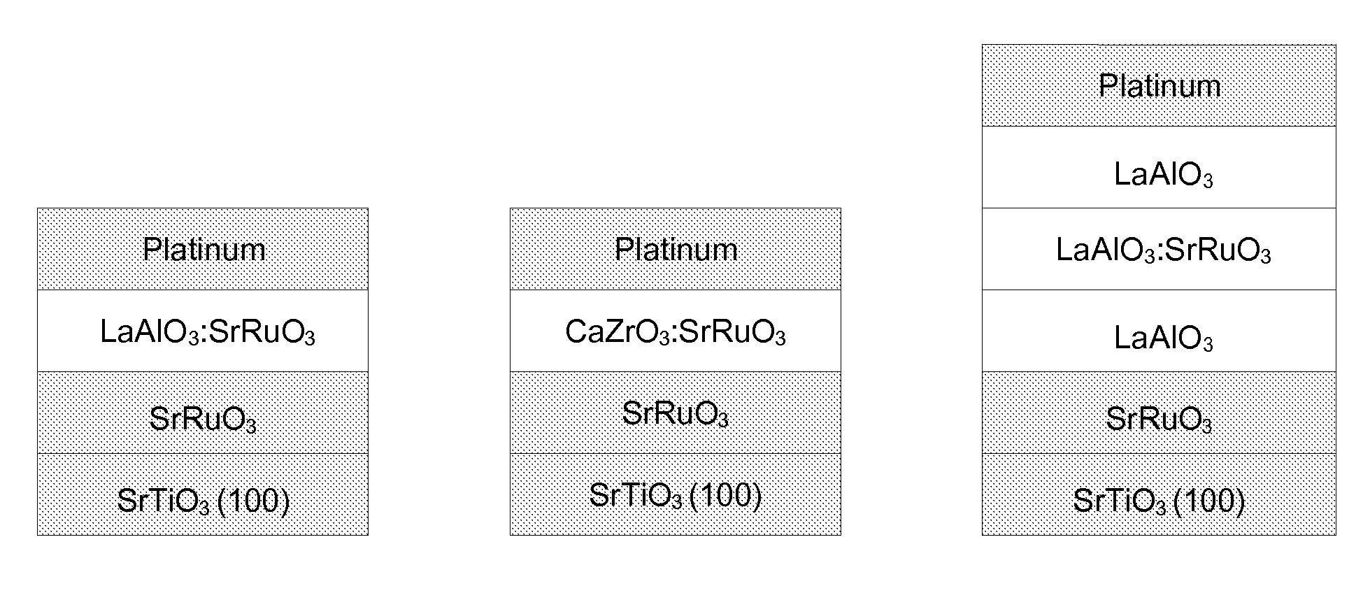
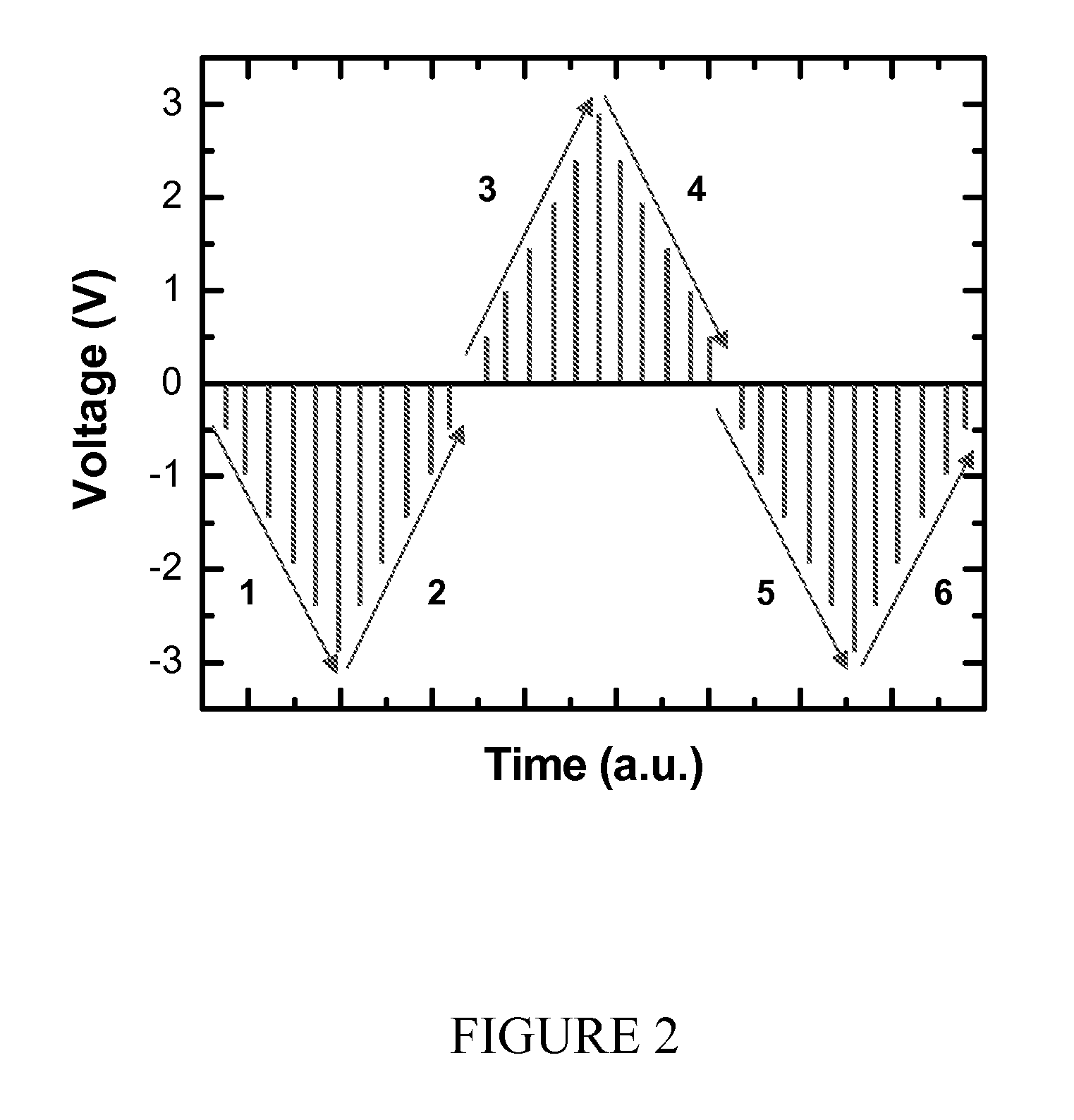
[0074]The present invention relates to two-point resistance-switching oxide layers, semiconductor devices incorporating same, and methods for making such oxide layers and devices. Resistance-switching oxide layers, and devices incorporating same, are suitable for various non-volatile memory applications. Under a resistance-switching regime, when an appropriate voltage pulse is applied, the resistance of the oxide layer can be increased and remain so until application of another appropriate voltage pulse, typically of the opposite polarity, which returns the resistance to the low value. Devices incorporating such resistance-switching oxide layers should be switchable at a modest voltage, preferably below about 3 V.

[0075]Resistance-switching oxide films, according to the certain preferred aspects of the present invention, include at least about 60 atomic percent of an insulator oxide matrix having a conducting material dopant in an amount up to about 40 atomic percent. The matrix (sol...


PUM

PropertyMeasurementUnit
total thicknessaaaaaaaaaa
thicknessaaaaaaaaaa
set-reset-voltageaaaaaaaaaa

Abstract

Non-volatile resistance-switching oxide films, and devices therewith, are disclosed. One embodiment of a suitable device is composed of a SRO-CZO thin film having a thickness of from about 6 to about 30 nm, and composed of from about 3 to about 10 molar % of a SrRuO3 conducting oxide dopant and from about 90 to about 97 molar % of a CaZrO3 insulating oxide material.

Description

CROSS-REFERENCE TO RELATED APPLICATIONS[0001]This application is a continuation-in-part of U.S. Ser. No. 11 / 291,945, “Resistance-Switching Oxide Thin Film Devices”, filed on Nov. 30, 2005, the entirety of which is incorporated by reference herein.STATEMENT OF GOVERNMENT INTERESTS[0002]The invention was made with U.S. Government support. The Government may have certain rights in the invention under National Science Foundation (NSF) Grant Nos. DMR03-03458 and DMR05-20020.FIELD OF THE INVENTION[0003]The invention generally relates to semiconductor devices, and more particularly to resistance-switching oxide semiconductor devices. The present invention also generally relates to resistance-switching oxide compositions and methods for making same.BACKGROUND OF THE INVENTION[0004]Materials exhibiting reversible resistance switching are attractive for many of today's semiconductor devices, including non-volatile random-access memory devices. However, previous efforts in the art to reversibl...

Claims


Application Information

Patent Timeline
Patent Type & Authority Patents(United States)
IPC IPC(8): B32B9/00C01F7/00C01G25/02C04B35/00
CPCC04B35/44C04B35/486C04B35/488C04B35/62218H01L29/0895H01L45/1233H01L45/147H01L45/1625H01L45/10C04B2235/3208C04B2235/3213C04B2235/3215C04B2235/3224C04B2235/3227C04B2235/3279C04B2235/3289H10N70/25H10N70/8836H10N70/026H10N70/826
Inventor CHEN, I-WEIWANG, YUDIKIM, SOO GIL
Owner THE TRUSTEES OF THE UNIV OF PENNSYLVANIA
Why Eureka
Try Eureka