Enhanced process yield using a hot-spot library

a technology of process yield and hot spot library, which is applied in the direction of semiconductor/solid-state device testing/measurement, instruments, semiconductor devices, etc., can solve the problems of chemical processes becoming more sensitive to defects or patterning errors, and achieve the effect of improving process yield

Inactive Publication Date: 2010-03-02
TOKYO ELECTRON LTD
View PDF21 Cites 27 Cited by
  • Summary
  • Abstract
  • Description
  • Claims
  • Application Information

AI Technical Summary

Benefits of technology

[0006]The invention can provide apparatus and methods of processing a substrate in real-time using hot-spot procedures, models, and libraries to improve process yield.

Problems solved by technology

Chemical processes become more sensitive to defects or patterning errors when pushed to the lithography limits.

Method used


Image

  • Enhanced process yield using a hot-spot library
  • Enhanced process yield using a hot-spot library
  • Enhanced process yield using a hot-spot library

Examples


Embodiment Construction

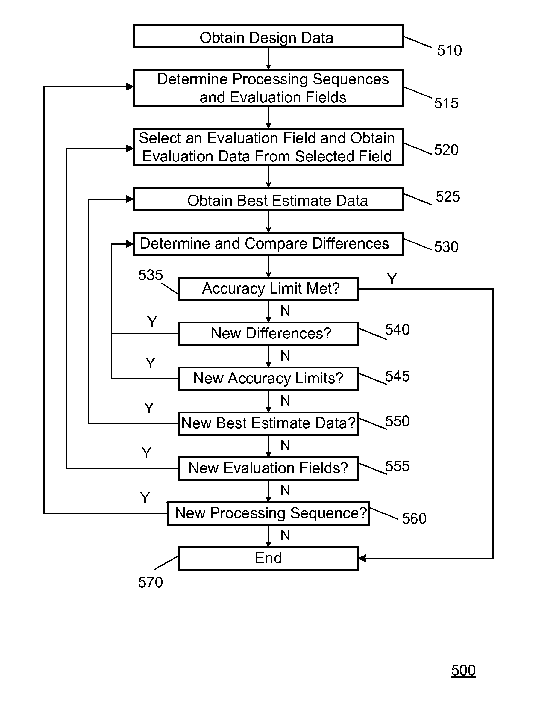
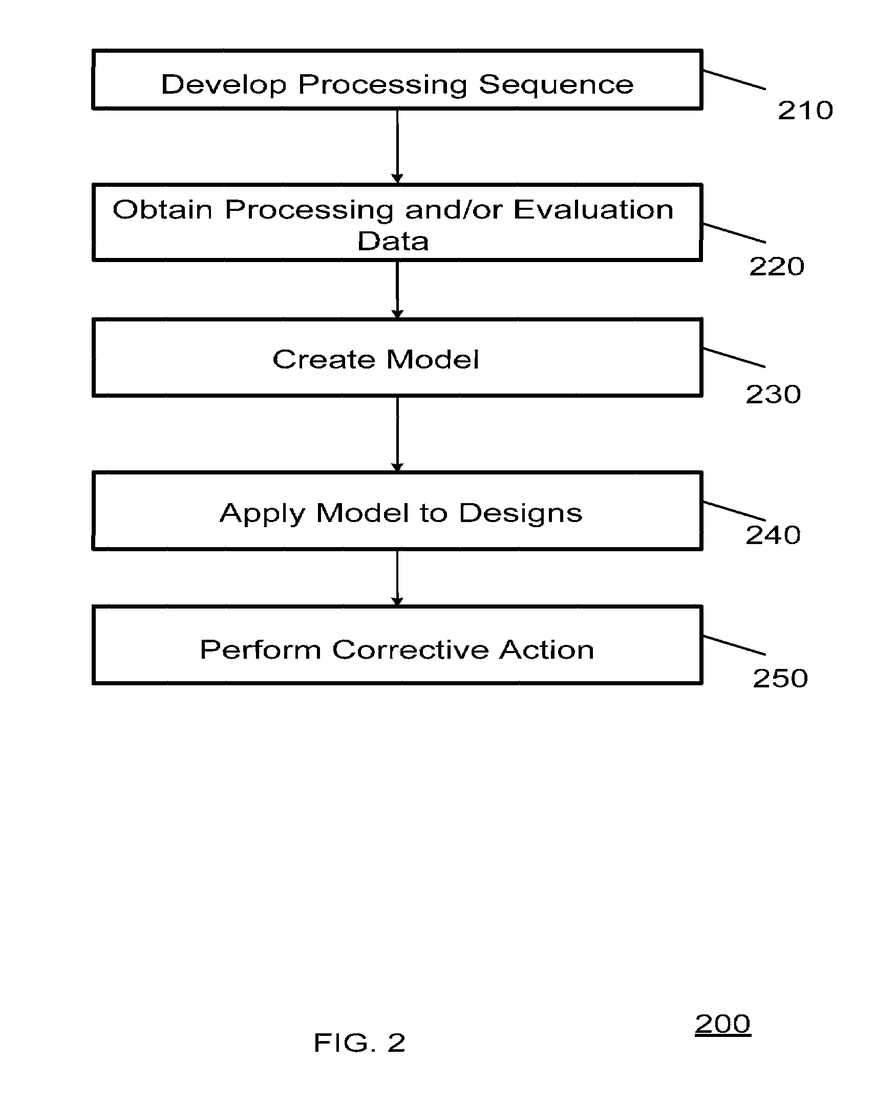
[0016]The invention provides apparatus and methods for processing substrates using process-related hot-spot libraries. The invention provides an Electronic Design Automation (EDA) methodology that correlates process-related hot-spots (resist bridging, watermark, etc) measured from a specific imaging / chemical process to simulated lithography contrast data, such as Normalized Image Log Slope (NILS) values. Simulated contrast data can be used to create, refine, and verify circuit design or layout rules for specific integrated circuit layers based on the predicted yield from calibrated hot-spot measurements.

[0017]In some embodiments, lithography simulation can be used to generate illumination conditions that stress the contrast data and corresponding process latitude, and the imaging illumination conditions can transition from poor contrast (image in resist NILS˜0.3) to good contrast (image in resist NILS>1). When process-related hot-spot library data is required, process experiments ca...


PUM


Abstract

The invention provides apparatus and methods for processing substrates using a hot-spot library.

Description

BACKGROUND OF THE INVENTION[0001]1. Field of the Invention[0002]The present invention relates to substrate processing, and more particularly to improving the process yield using hot-spot procedures and data.[0003]2. Description of the Related Art[0004]Many multiple patterning techniques are currently being use during semiconductor substrate processing to increase the number of features and / or structures within devices on a substrate. Multiple patterning techniques can include double exposure techniques, double patterning techniques, spacer techniques, mask techniques, and brute force techniques. In 2006, the International Technology Roadmap for Semiconductors roadmap was expanded to include double patterning a potential solution for 32 nm lithography. Multiple patterning techniques are viewed as some device manufacturers as bridge solutions that can be used until Extreme Ultra-Violet (EUV) techniques become more fully developed.[0005]Integrated Circuit (IC) design shrinks push the l...

Claims


Application Information

Patent Timeline
Patent Type & Authority Patents(United States)
IPC IPC(8): G06F17/50
CPCH01L22/20H01L2924/0002H01L2924/00
Inventor RATHSACK, BENJAMEN M.NAFUS, KATHLEENSCHEER, STEVEN
Owner TOKYO ELECTRON LTD
Why Eureka
Try Eureka