Method and system for microfluidic device and imaging thereof

a microfluidic device and imaging technology, applied in the field of microfluidic systems, can solve the problems of limited bulk and surface micro-machining methods, large and complex designs, and certain limitations of conventional mems structures and techniques, and achieve the effect of a wider range of applicability

Inactive Publication Date: 2010-04-13
FLUIDIGM CORP
View PDF115 Cites 73 Cited by
  • Summary
  • Abstract
  • Description
  • Claims
  • Application Information

AI Technical Summary

Benefits of technology

[0029]Numerous benefits are achieved using the present invention over conventional techniques. Some embodiments provide alignment and / or focus based on mapping between the design space and the measurement space. The transformation between the design space and the measurement space uses, for example, at least three fiducial markings. Certain embodiments provide accurate focusing by acquiring and analyzing a plurality of images along at least one dimension. Some embodiments of the present invention perform alignment and focusing on a microfluidic device including at least one flexible substrate. The alignment and focusing take into account the deformation of the flexible substrate. Certain embodiments improve throughput in imaging system. For example, the imaging system uses a computer system to automatically perform alignment and focusing. In another example, mapping from the design space to the measurement space increases the accuracy of stage positioning, and thereby, the efficiency of high-resolution image acquisition. Depending upon the embodiment, one or more of these benefits may exist. These and other benefits have been described throughout the present specification and more particularly below.

Problems solved by technology

Unfortunately, certain limitations exist with these conventional MEMS structures and techniques for making them.
As merely an example, a limitation of silicon-based micro-machining is that the stiffness of the semiconductor materials used necessitates high actuation forces, which result in large and complex designs.
In fact, both bulk and surface micro-machining methods are often limited by the stiffness of the materials used.
Additionally, adhesion between various layers of the fabricated device is also a problem.
On the other hand, when surface micro-machining, thermal stresses between the various layers of the device limits the total device thickness, often to approximately 20 microns.
In practice however, forming a high quality crystal is generally difficult, often requiring much trial and error and patience on the part of the researcher.
Specifically, the highly complex structure of even simple biological compounds means that they are usually not amenable to forming a highly ordered crystalline structure.

Method used


Image

  • Method and system for microfluidic device and imaging thereof
  • Method and system for microfluidic device and imaging thereof
  • Method and system for microfluidic device and imaging thereof

Examples


Embodiment Construction

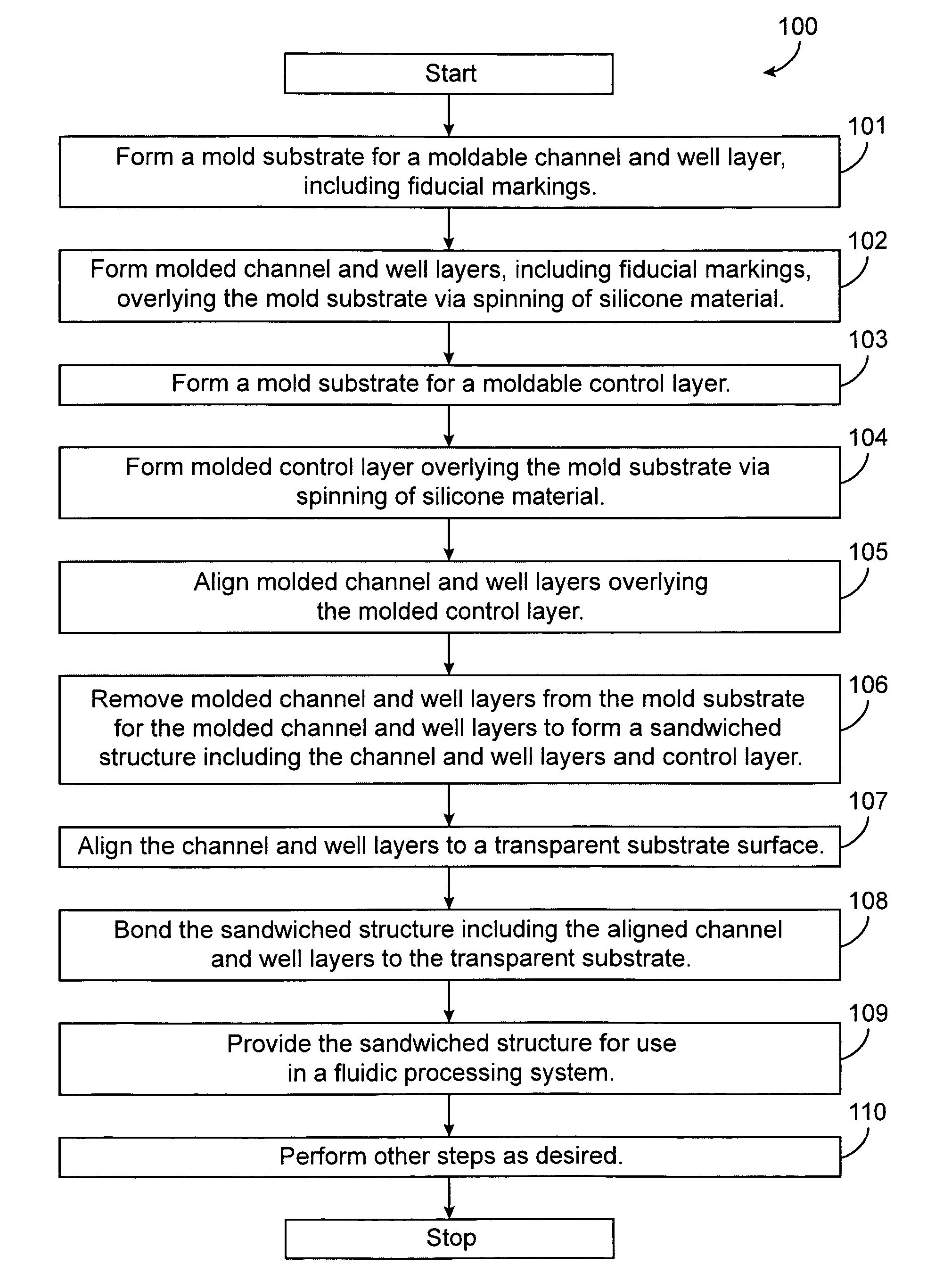
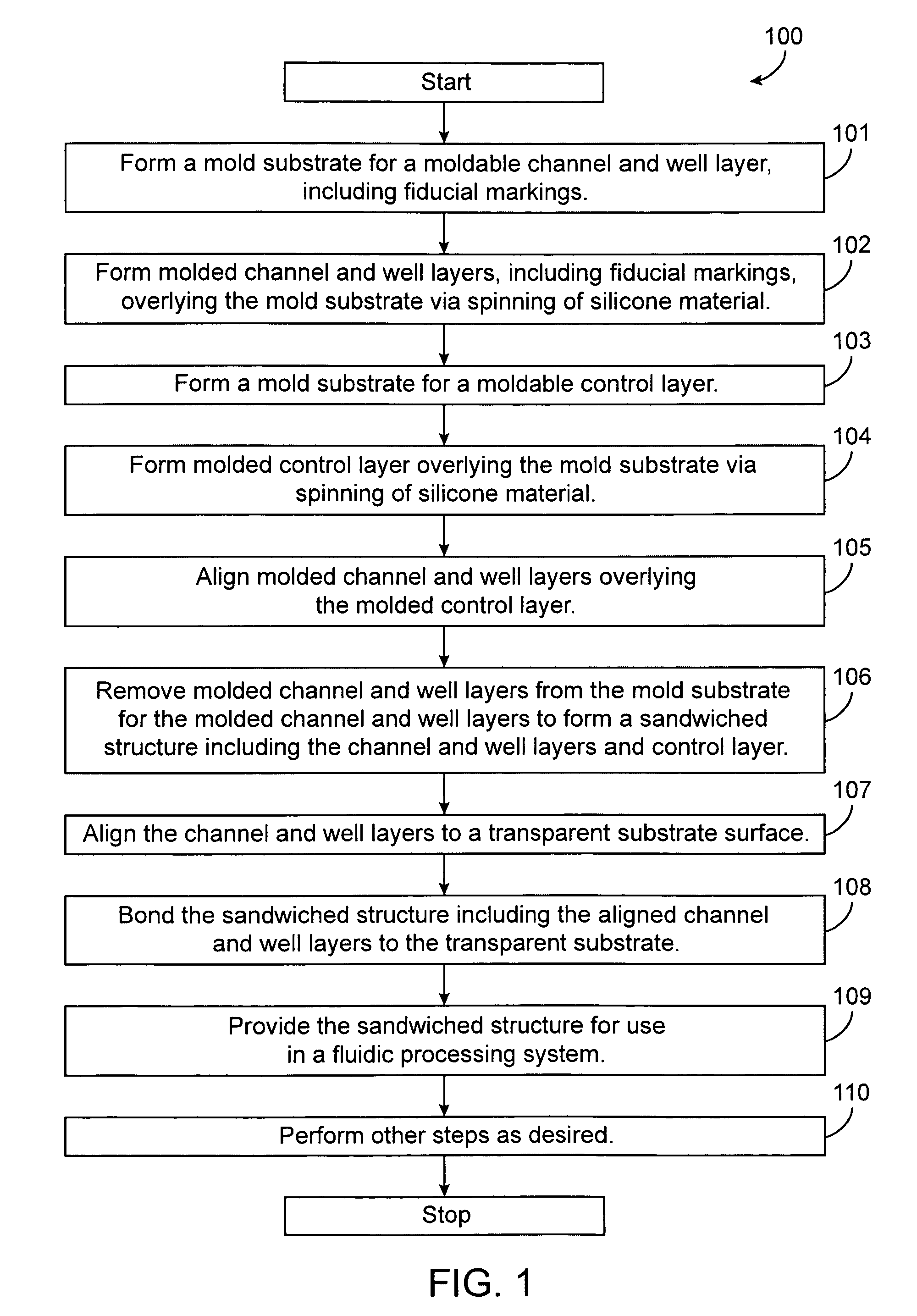
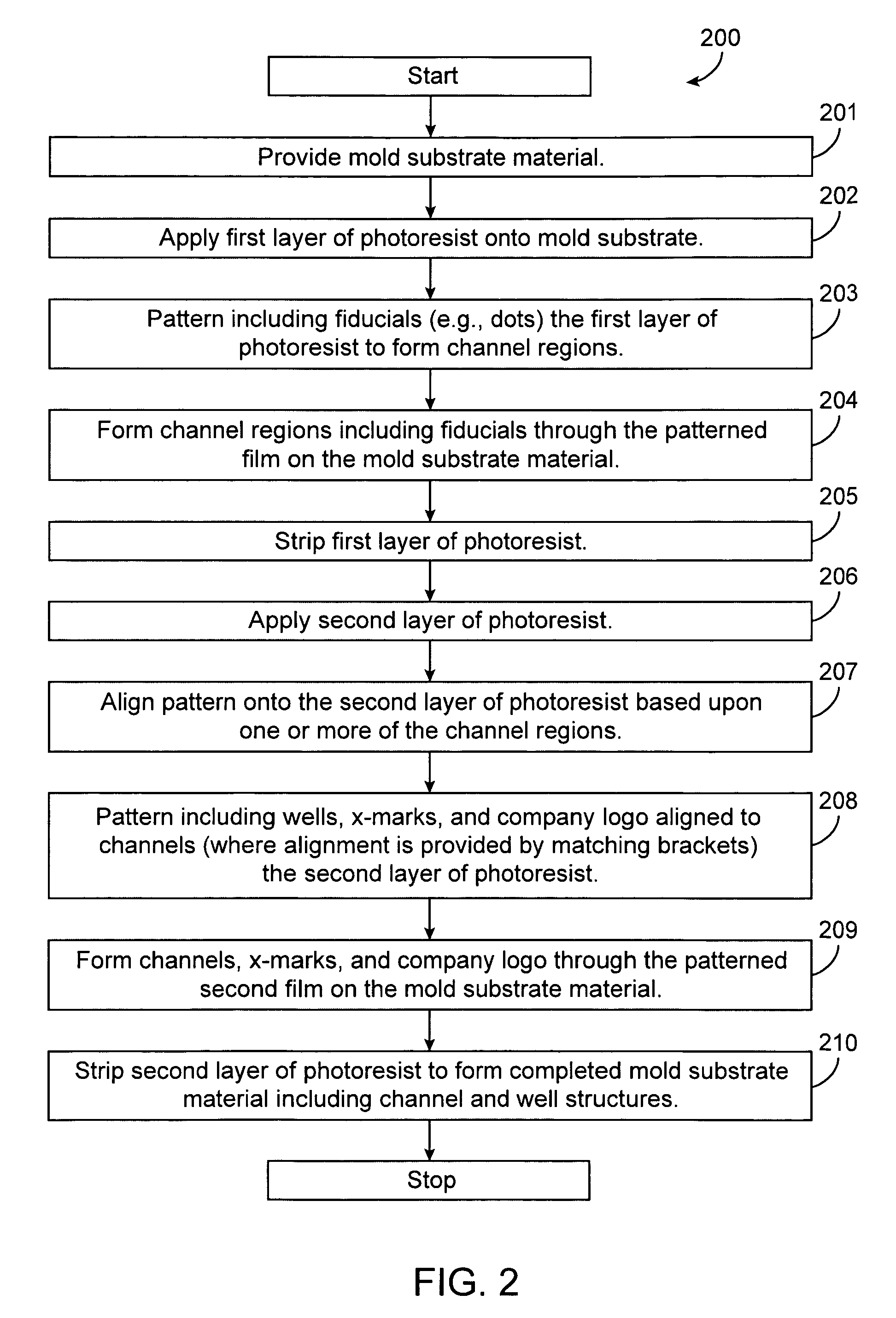
[0053]According to the present invention, techniques for microfluidic systems, including a microfluidic chip or circuit, are provided. More particularly, the invention provides a microfluidic structure and method of manufacture, and a system and method for imaging a microfluidic device. Merely by way of example, the fiducial markings are used for processing and imaging a microfluidic chip, but it would be recognized that the invention has a much broader range of applicability.

Method for Manufacturing Fluidic Chip

[0054]A method for manufacturing a fluidic chip according to an embodiment of the present invention may be outlined below. Certain details of the method 100 are also provided according to a flow diagram illustrated by FIG. 1, which is not intended to unduly limit the scope of the claims herein. One of ordinary skill in the art would recognize many variations, alternatives, and modifications.

[0055]1. Form a mold substrate for a moldable channel and well layer 101, including f...


PUM

PropertyMeasurementUnit
thicknessaaaaaaaaaa
widthaaaaaaaaaa
widthaaaaaaaaaa

Abstract

A biological substrate, e.g., microfluidic chip. The substrate includes a rigid substrate material, which has a surface region capable of acting as a handle substrate. The substrate also has a deformable fluid layer coupled to the surface region. One or more well regions are formed in a first portion of the deformable fluid layer and are capable of holding a fluid therein. The one or more channel regions are formed in a second portion of the deformable fluid layer and are coupled to one or more of the well regions. An active region is formed in the deformable fluid layer. At least three fiducial markings are formed within the non-active region and disposed in a spatial manner associated with at least one of the well regions. A control layer is coupled to the fluid layer.

Description

CROSS-REFERENCES TO RELATED APPLICATIONS[0001]This application claims priority to U.S. Provisional Patent Application Nos. 60 / 472,226 filed May 20, 2003, 60 / 490,666 filed Jul. 28, 2003, and 60 / 490,584 filed Jul. 28, 2003, all of which are commonly assigned and incorporated by reference herein for all purposes.STATEMENT AS TO RIGHTS TO INVENTIONS MADE UNDER FEDERALLY SPONSORED RESEARCH AND DEVELOPMENT[0002]Not Applicable.REFERENCE TO A “SEQUENCE LISTING,” A TABLE, OR A COMPUTER PROGRAM LISTING APPENDIX SUBMITTED ON A COMPACT DISK[0003]Not Applicable.BACKGROUND OF THE INVENTION[0004]According to the present invention, techniques for microfluidic systems, including a microfluidic chip or circuit, are provided. More particularly, the invention provides a microfluidic structure and method of manufacture, and a system and method for imaging a microfluidic device. Merely by way of example, the fiducial markings are used for processing and imaging a microfluidic chip, but it would be recogn...

Claims


Application Information

Patent Timeline
Patent Type & Authority Patents(United States)
IPC IPC(8): G01N33/00B01L3/00
CPCB01L3/5025B01L3/502707B01L2200/025B01L2200/12B01L2300/0816Y10T436/11B01L2300/0867B01L2300/087B01L2300/0887B01L2400/0481B01L2400/0655B01L2300/0864G01N33/00
Inventor QUAN, EMERSON CHUENGTAYLOR, COLIN JONLEE, MICHAELCESAR, CHRISTOPHER G.HARRIS, GREGSUN, GANG
Owner FLUIDIGM CORP
Why Eureka
Try Eureka