

Display device and driving method of the same
a technology of image display and driving method, which is applied in the direction of electric digital data processing, instruments, computing, etc., can solve the problems of sacrificing the gray-scale characteristics of images and unable to obtain predetermined gray-scales
- Summary
- Abstract
- Description
- Claims
- Application Information
AI Technical Summary
Benefits of technology
Problems solved by technology
Method used
Image

Examples
embodiment 1
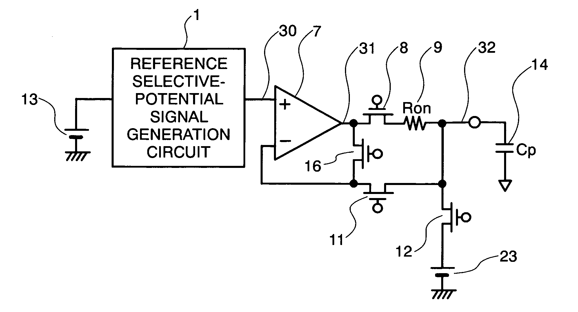
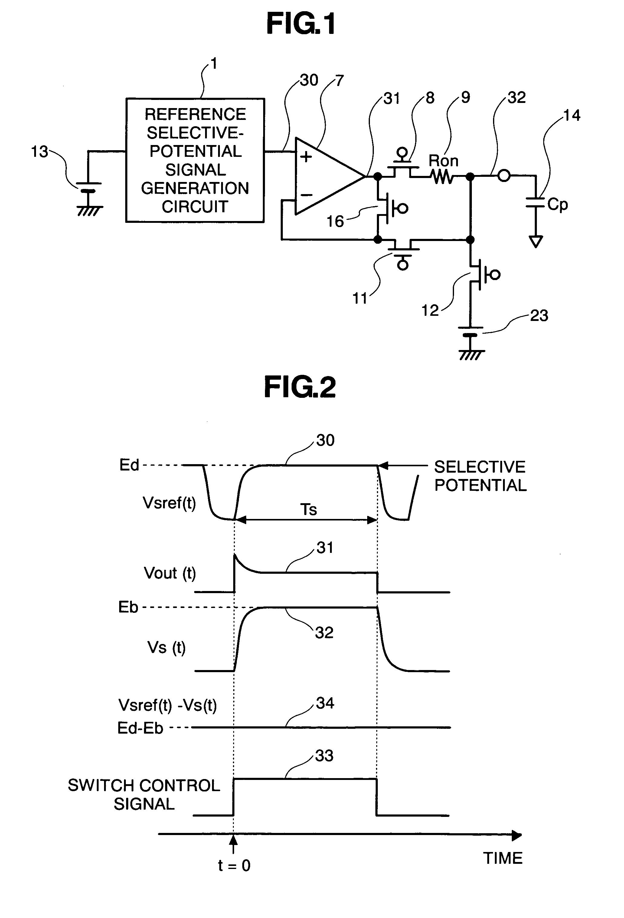
[0069]Hereinafter, an image display device according to embodiment 1 of the invention is described. FIG. 1 shows a block diagram of the embodiment, and FIG. 2 shows an operation waveform diagram for illustrating operation in a configuration of FIG. 1.
[0070]In FIG. 1, the reference voltage source 13 is a voltage source that determines scan selection potential, which is inputted into a reference-selection-potential-signal generation circuit 1. An output signal of the reference-selection-potential-signal generation circuit 1 gradually rises at the beginning of a selection period of horizontal scan.
[0071]An output signal 30 of the reference-selection-potential-signal generation circuit 1 is shown as a delayed waveform 30 in FIG. 2. The output signal 30 is applied to a positive-phase input terminal as a reference signal input terminal of the amplifier 7 as a scan-electrode potential correction unit to be into a reference signal in selection of a scan line.
[0072]An output terminal of the ...
embodiment 2
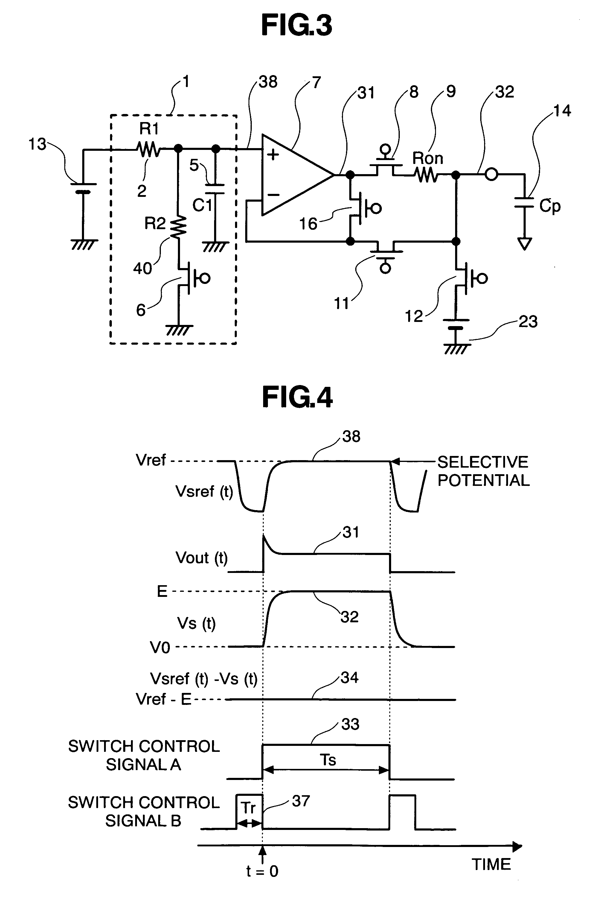
[0085]Hereinafter, another embodiment of an image display device according to the invention is described using FIG. 3 and FIG. 4. FIG. 3 is a circuit block diagram of the embodiment, and FIG. 4 is an operation waveform diagram for describing operation in a configuration of FIG. 3.
[0086]In FIG. 3, the output terminal of the reference voltage source 13 is connected with the resistor 2 having a resistance value R1, and the capacitor 5 having a capacitance value C1 is connected between one end of the resistor 2 and ground. The resistor 40 having a resistance value R2 is connected to a connection point between the resistor 2 and the capacitor 5, and the switch 6 is connected in series with the resistor 40, which is further connected to ground.
[0087]A waveform 33 in FIG. 4 is a switch control signal A for controlling on-and-off of the scan selection switch 8 and the feedback switch 11, and polarity is assumed such that when the switch control signal A is in the high level, the scan select...
embodiment 3
[0110]Hereinafter, still another embodiment of an image display device of the invention is described using FIG. 5 and FIG. 6. FIG. 5 is a circuit block diagram of the embodiment, and FIG. 6 is an operation waveform diagram for describing operation in a configuration of FIG. 5.
[0111]In FIG. 5, the output terminal of the reference voltage source 13 is connected with the resistance 2 having the resistor value R1, and the capacitor 5 having the capacitance value C1 is connected between one end of the resistor 2 and ground. The switch 35 is connected to the connection point between the resistor 2 and the capacitor 5, and the voltage source 36, and the voltage source 36 is connected to ground.
[0112]The switches 35 and 16 are driven by the switch control signal B, which are on in the high level.
[0113]The time t35 and 16 are on, wherein the output voltage of the amplifier 7 is returned into the negative-phase input terminal of the amplifier 7. Therefore, the output voltage of the amplifier ...
PUM
 Abstract
Description
Claims
Application Information