Power-on reset circuit using flip-flop and semiconductor device having such power-on reset circuit

a technology of flip-flops and reset circuits, applied in electronic switching, pulse automatic control, pulse technique, etc., to achieve the effect of being particularly effective and more reliable in initialization

Inactive Publication Date: 2010-04-20
LONGITUDE SEMICON S A R L
View PDF19 Cites 6 Cited by
  • Summary
  • Abstract
  • Description
  • Claims
  • Application Information

AI Technical Summary

Benefits of technology

[0020]In the power-on reset circuit according to the present invention, the plurality of dummy flip-flops are configured to have a characteristic of being easy to be shifted to the reset state that is equivalent to that of the setting flip-flop.
[0022]In the power-on reset circuit according to the present invention, the dummy flip-flop is configured to have a characteristic of being easy to be shifted to the reset state that is equivalent to that of the setting flip-flop, and upon receiving a different set signal at the set terminal thereof, the dummy flip-flop outputs a different latch signal.
[0023]In the power-on reset circuit according to the present invention, the setting flip-flop is configured as a symmetrical flip-flop, while the dummy flip-flop is configured as an asymmetrical flip-flop which is easy to be shifted to a direction in which the latch signal is reset to the inactive level at power-on.
[0025]The power-on reset circuit according to the present invention has a dummy flip-flop in addition to a setting flip-flop. Even if initialization is not performed by a power-on reset signal at power-on, resetting and the initialization can be performed by using output from the dummy flip-flop. The power-on reset circuit according to the present invention is particularly effective when used in a mode setting latch circuit of a semiconductor device. For example, it is usable in a mode register of a DRAM which is a semiconductor memory device. EMRS 1 (Extended Mode Register 1) of a DDRII DRAM has settings for the OCD drive mode. If the OCD drive mode is erroneously entered at power-on, the output becomes Low-Z. The present invention, when applied to such a latch circuit, is capable of avoiding these problems liable to occur at power-on. The provision of a dummy flip-flop makes it possible to provide a power-on reset circuit and a semiconductor device capable of more reliable initialization at power-on.

Problems solved by technology

The aforementioned semiconductor devices have a problem that initialization by a power-on reset signal cannot be performed successfully at power-on so that a latch signal is set to a mode different from an expected value, leading to malfunction.

Method used


Image

  • Power-on reset circuit using flip-flop and semiconductor device having such power-on reset circuit
  • Power-on reset circuit using flip-flop and semiconductor device having such power-on reset circuit
  • Power-on reset circuit using flip-flop and semiconductor device having such power-on reset circuit

Examples


first embodiment

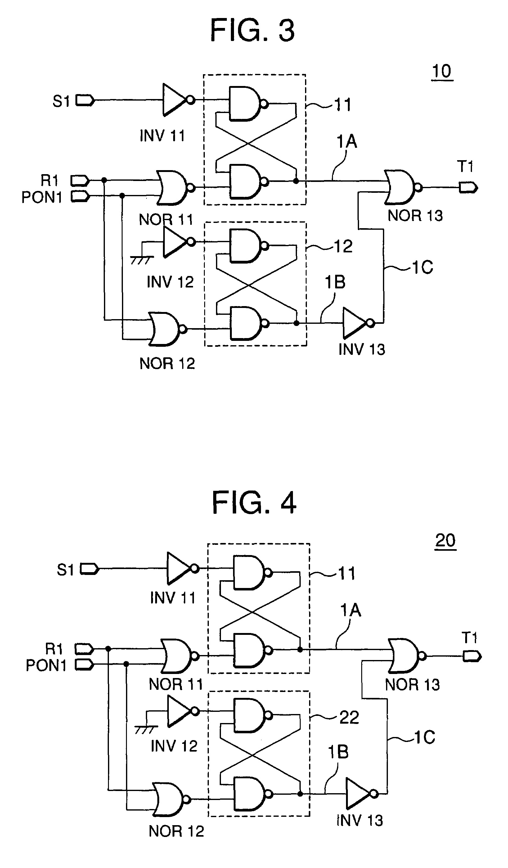
[0035]A first embodiment of the present invention will be described with reference to FIGS. 3 and 4. FIGS. 3 and 4 show a power-on reset circuit using a flip-flop. A power-on reset circuit 10 shown in FIG. 3 is composed of flip-flops 11 and 12, inverter circuits INV11, INV12 and INV13, and NOR circuits NOR11, NOR12 and NOR13. A power-on reset circuit 20 shown in FIG. 4 has same configuration as that of the power-on reset circuit 10 except that the flip-flop 12 of the power-on reset circuit 10 of FIG. 3 is replaced with a flip-flop 22.

[0036]The flip-flop 11 in the power-on reset circuit 10 receives, as set input, a set signal S1 after being inverted by the inverter circuit INV11. The flip-flop 11 receives, as reset input, an output signal from the NOR circuit NOR11 receiving a reset signal R1 and a power-on reset signal PON1 as input. The flip-flop 12 receives, as set input, output from the inverter circuit INV12 receiving an input signal having ground potential. The flip-flop 12 rec...

second embodiment

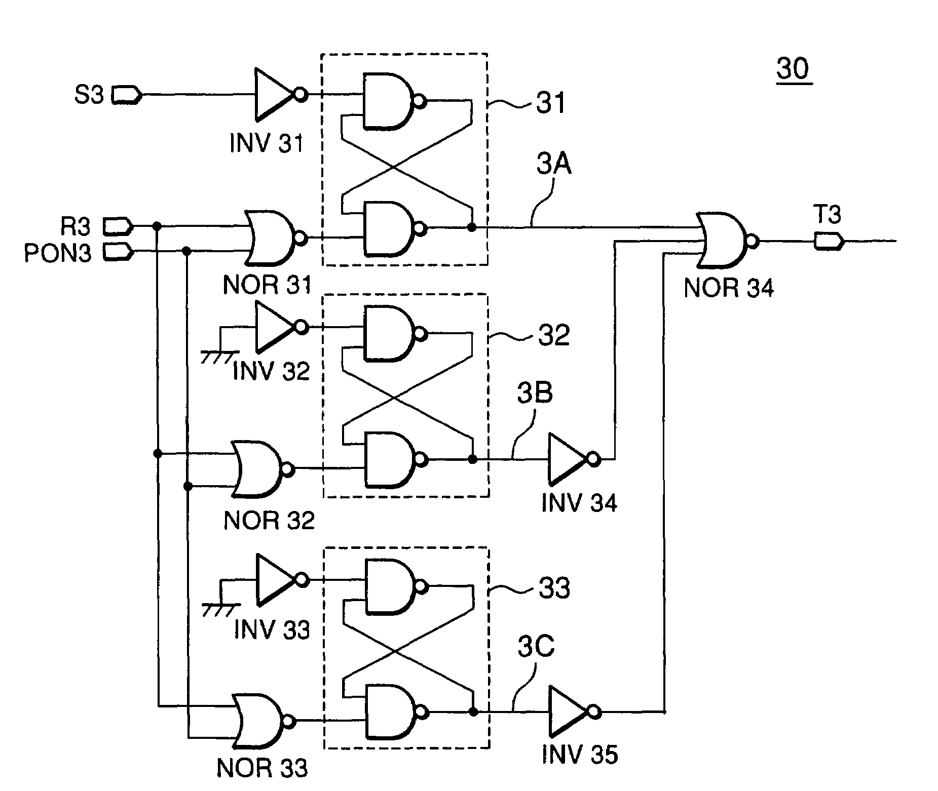
[0051]A second embodiment of the present invention will be described with reference to FIGS. 5 and 6. In this embodiment, the dummy flip-flop according to the first embodiment is multiplexed, and two dummy flip-flops are provided. FIG. 5 shows a first multiplexed power-on reset circuit 30, while FIG. 6 shows a modification thereof, a second multiplexed power-on reset circuit 30-1. The power-on reset circuit 30 shown in FIG. 5 is composed of a setting flip-flop 31, dummy flip-flops 32 and 33, inverter circuits INV31, INV32, INV33, INV34, and INV35, NOR circuits NOR31, NOR32, NOR33, and NOR34. The power-on reset circuit 30-1 shown in FIG. 6 has dummy flip-flops 34 and 35 in place of the dummy flip-flops 32 and 33 of FIG. 5, while the other configuration is the same as the power-on reset circuit 30.

[0052]The setting flip-flop 31 of the power-on reset circuit 30 receives, as set input, a set signal S3 after being inverted by the inverter circuit INV31. The setting flip-flop 31 receives,...

third embodiment

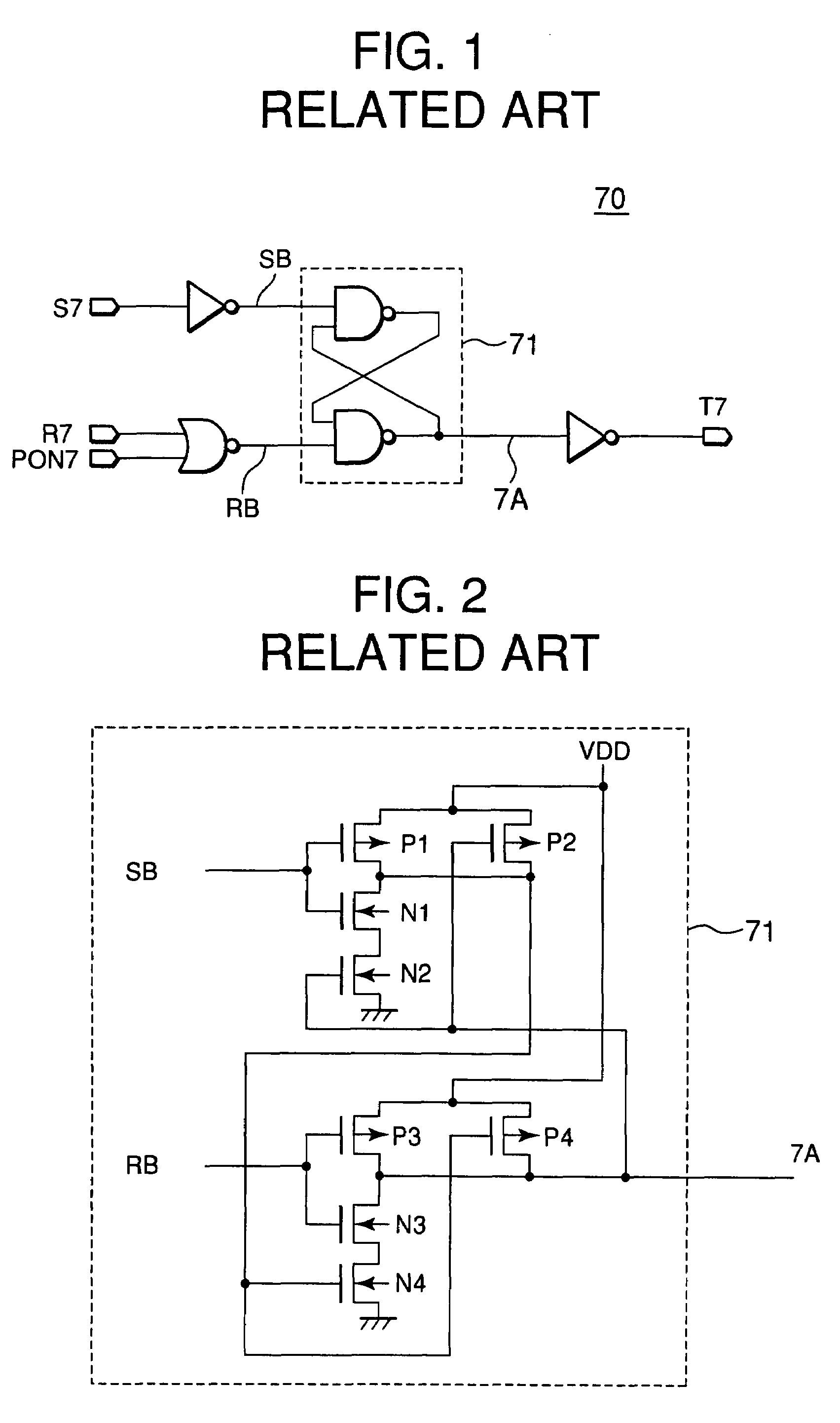
[0064]A third embodiment of the present invention will be described with reference to FIGS. 7 and 8. According to this embodiment, a flip-flop of a power-on reset circuit generating another latch signal is utilized as a dummy flip-flop. FIG. 7 shows a power-on reset circuit 50, while FIG. 8 shows a modification thereof, a power-on reset circuit 50-1.

[0065]In the first and second embodiments described above, the latch signal is set to an expected value at power-on by adding the dummy flip-flop. It is also described that the effect is enhanced as the number of the dummy flip-flops is increased. However, the increase of the number of the dummy flip-flops obviously leads to the increase of the chip surface area. The third embodiment relates to configuration for avoiding this. According to the third embodiment, latch signals T5A and T5B are output from flip-flops 51 and 52 and latch separate commands, respectively. These latch signals T5A and T5B are selected such that they are not activ...


PUM


Abstract

A power-on reset circuit has a dummy flip-flop in addition to a setting flip-flop. Even if resetting is not performed by a power-on reset signal at power-on, output from the dummy flip-flop is used to perform resetting and initialization.

Description

[0001]This application claims priority to prior Japanese patent application JP2006-108762, the disclosure of which is incorporated herein by reference.BACKGROUND OF THE INVENTION[0002]The present invention relates to a power-on reset circuit for use in a semiconductor device, particularly to a power-on reset circuit for preventing malfunction of a semiconductor device at power-on, and also relates to a semiconductor device having such a power-on reset circuit.[0003]Recent semiconductor devices, which have been sophisticated and systematized, incorporate many functions. In order to have these functions work correctly according to commands from the outside, the commands must be held. A latch circuit such as a flip-flop is mainly used to store command information externally input, and internal circuit operation is controlled according to the stored command information. The latch circuit such as a flip-flop is initialized to a reset state by using a power-on reset signal at power-on to ...

Claims


Application Information

Patent Timeline
Patent Type & Authority Patents(United States)
IPC IPC(8): H03L7/00
CPCH03K17/22
Inventor MAEDA, KAZUNORI
Owner LONGITUDE SEMICON S A R L
Why Eureka
Try Eureka