Force sensor chip

a technology of force sensor and sensor chip, which is applied in the direction of stringed rackets, instruments, force/torque/work measurement apparatus, etc., can solve the problems of irregular initial resistance values (resistance values) of strain resistance elements, and achieve the effect of high accuracy

Active Publication Date: 2010-05-04
HONDA MOTOR CO LTD
View PDF25 Cites 9 Cited by
  • Summary
  • Abstract
  • Description
  • Claims
  • Application Information

AI Technical Summary

Benefits of technology

[0014]An object of the present invention is to provide a force sensor chip in which the temperature-compensating resistance elements are subjected to the same level of heat-related effects as the strain resistance elements; are not affected by stress from externally applied forces; and are able to have heat transfer characteristics (substrate radiation properties) that are of the same level as where the strain resistance elements are disposed. Temperature compensation can be performed with high accuracy, and stress can be detected with high accuracy.
[0015]Another object of the present invention is to provide a force sensor chip in which the initial resistance values of the strain resistance elements can be optimized in consideration of the crystal orientation of the semiconductor substrate, the outputs across the axes can be properly balanced, and stress can be detected with high accuracy.
[0023]In the force sensor chip thus arranged, the temperature-compensating resistance elements are placed in the vicinity of the strain resistance elements, and both are readily affected by the temperature to a similar degree. Moreover, since the structure in the periphery of the locations where the strain resistance elements are disposed is the same as the structure in the periphery of the locations where the temperature-compensating resistance elements are disposed, the structure in the periphery of the locations where the temperature-compensating resistance elements are disposed will not deform under the stress caused by external forces, and can be subjected to the effect caused by heat emitted from the semiconductor plate (temperature effect) to the same degree as the strain resistance element. Furthermore, the temperature-compensating resistance elements and the strain resistance elements will also be equally subjected to the effect caused by micro-deformation of the substrate due to the effect of the heat, thereby allowing high-accuracy temperature compensation to be performed, and allowing the strain resistance elements to be able to output accurate detection values corresponding only to stress. The force sensor chip of the present invention can thereby detect stress with a very high degree of accuracy.
[0027]In the force sensor chip according to the second aspect, the base member is thus formed using a semiconductor substrate having a crystal orientation, and the initial resistance values of the plurality of strain resistance elements formed on the base member are set to different values in consideration of the crystal orientation in accordance with each of two perpendicular axes on the surface of the base member. Therefore, the initial resistance values of the strain resistance elements (which may include the temperature-compensating resistance elements) are optimized the output across the axes can be satisfactorily balanced, and stress can be detected with high accuracy.

Problems solved by technology

However, even when the temperature-compensating resistance elements are provided to locations where the temperature conditions are the same as those where the strain resistance elements are disposed (non-deforming regions), the initial resistance values (resistance values when no load is present) of the strain resistance elements will actually be irregular.
As a result, a problem occurs in that optimal values will not necessarily be obtained even when the temperature-compensating resistance elements are used to perform temperature compensation on the output values of the strain resistance elements.
However, this document does not disclose the concept of determining the layout of the resistance elements in consideration of the crystal orientation from the standpoint of properly balancing the outputs across the axes.

Method used


Image

  • Force sensor chip
  • Force sensor chip
  • Force sensor chip

Examples


Embodiment Construction

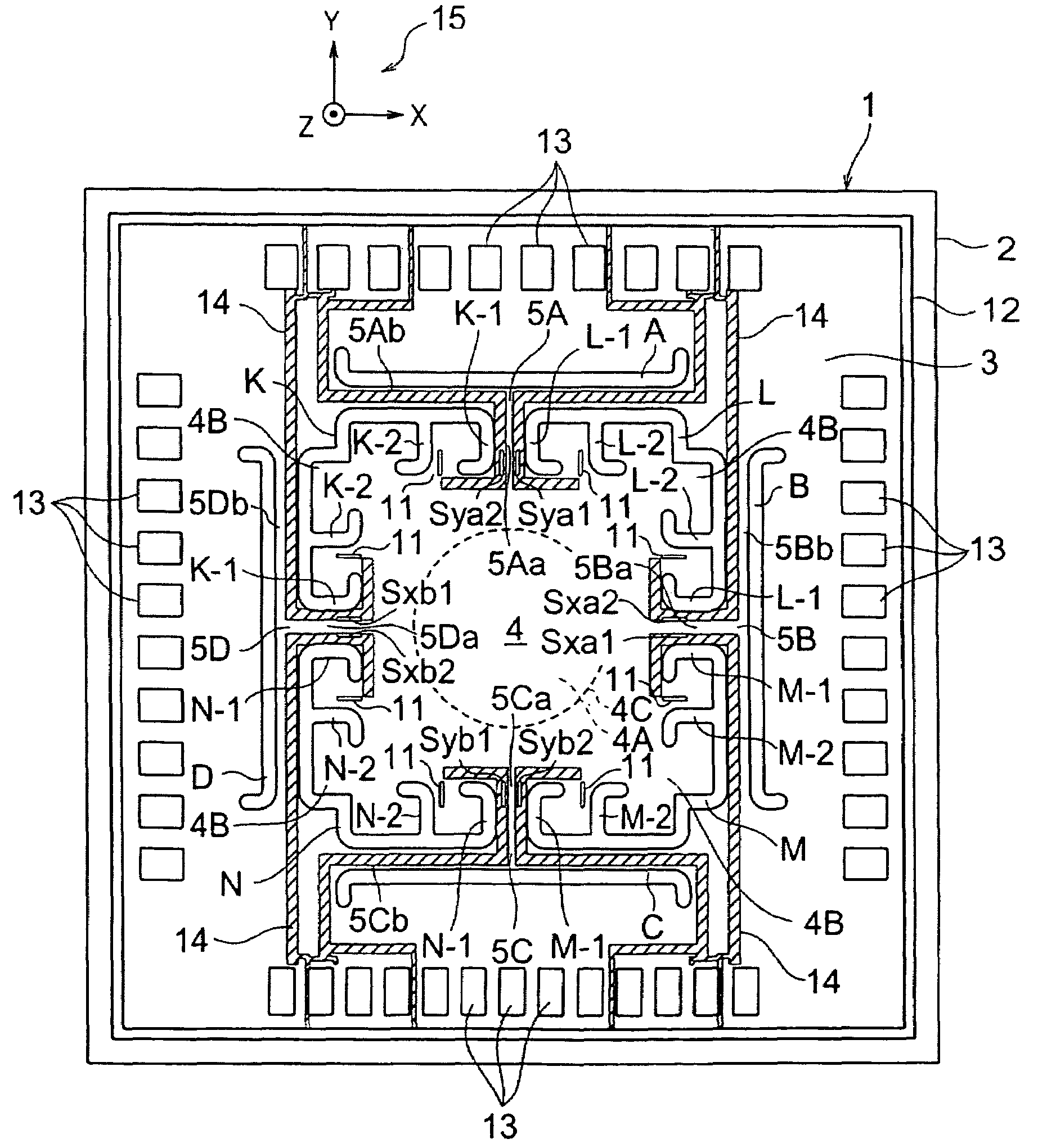
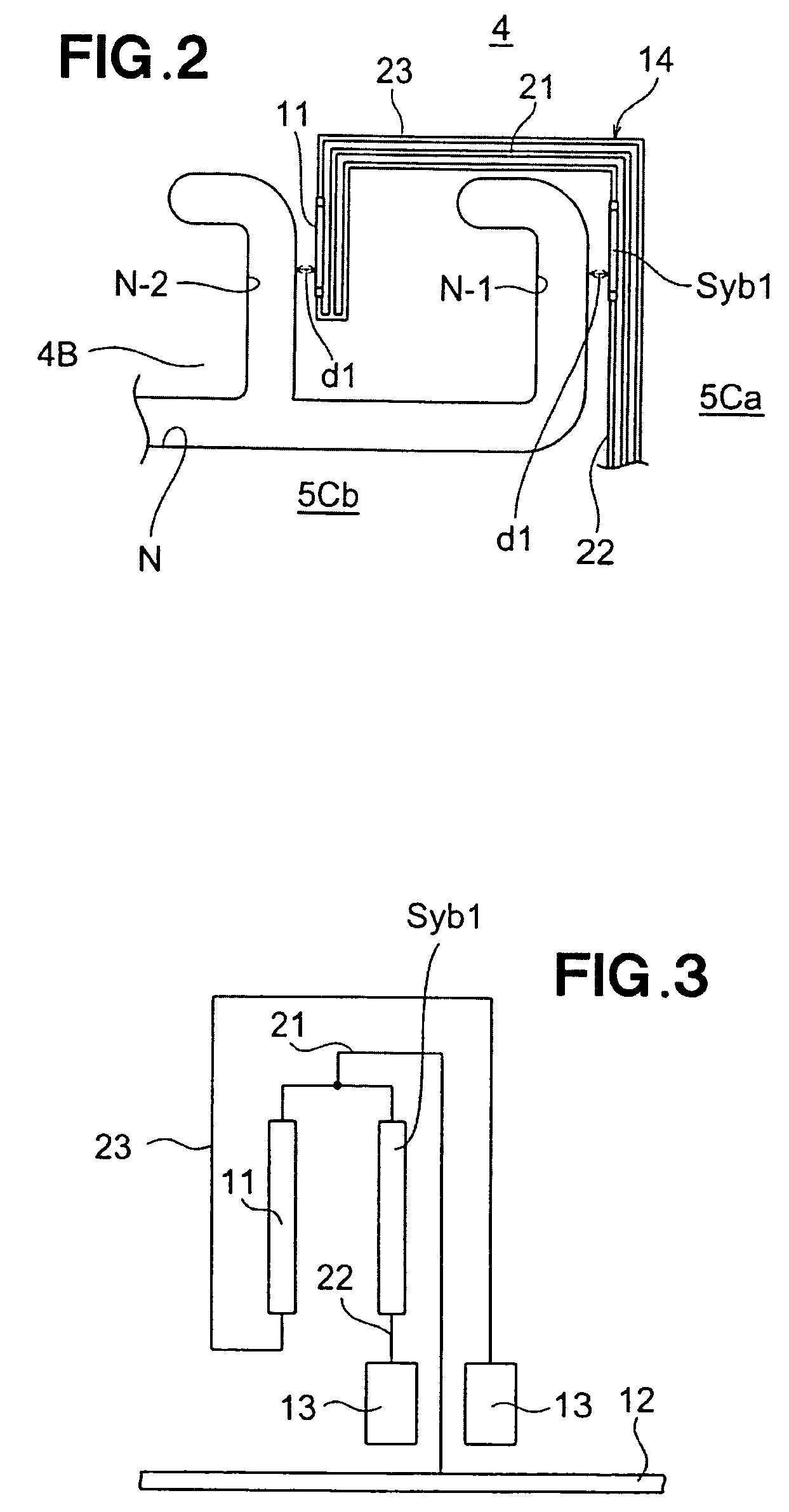
[0035]A typical embodiment of a force sensor chip according to the present invention will be described with reference to FIGS. 1 through 5. In this embodiment, a six-axis force sensor chip is given as an example of a force sensor chip. The force sensor chip of the present invention is not limited to a six-axis force sensor chip.

[0036]In FIG. 1, a six-axis force sensor chip 1 of the present embodiment is formed by a semiconductor substrate 2 that preferably has a square shape as viewed from above. The length of one side of the square semiconductor substrate 2 is, e.g., 5.5 mm. The substrate is not limited to a semiconductor substrate. The entirety of the six-axis force sensor chip 1 assumes the shape of a plate based on the semiconductor substrate 2.

[0037]When a semiconductor device is formed on the substrate 2, the six-axis force sensor chip 1 is preferably manufactured by forming holes and wires using a semiconductor manufacturing process technique (e.g., photolithography, ion impl...


PUM

PropertyMeasurementUnit
lengthaaaaaaaaaa
stressaaaaaaaaaa
external forceaaaaaaaaaa

Abstract

A force sensor chip including a semiconductor substrate having a plurality of strain resistance elements and temperature-compensating resistance elements corresponding to the resistance elements is disclosed. The structure in the periphery of parts where the strain resistance elements, which are provided to deforming parts in the action part formed on the semiconductor substrate, are disposed is the same as the structure in the periphery of parts where the temperature-compensating resistance elements in the action part are disposed.

Description

FIELD OF THE INVENTION[0001]The present invention relates generally to a force sensor chip and, more particularly, to a force sensor chip that has strain resistance elements formed on a semiconductor substrate using a semiconductor manufacturing process technique, and is used as a force sensor in a machine tool, pointing device or the like.BACKGROUND OF THE INVENTION[0002]In machine tools and other automated machinery, the work operation involves a force being applied to an object that is to be worked, or a force being received from an external source. In such cases, automated machines require that the moment and external force applied thereto be detected, and a control corresponding to the force and moment be carried out. The external force and moment must be accurately detected in order to carry out the control corresponding to the force and moment with high accuracy.[0003]In view of this, a variety of force sensors have been proposed in the past. Using the detection method as a b...

Claims


Application Information

Patent Timeline
Patent Type & Authority Patents(United States)
IPC IPC(8): G01L1/22G01D7/00
CPCG01L5/162G01L1/2281
Inventor SAKURAI, NOBUHIROOHSATO, TAKESHI
Owner HONDA MOTOR CO LTD
Why Eureka
Try Eureka