Process for producing electroluminescent element

a technology of electroluminescent elements and process steps, which is applied in the manufacture of electrode systems, electric discharge tubes/lamps, instruments, etc., can solve the problems of adversely affecting and achieve the effect of improving the luminescence efficiency of el elements

Inactive Publication Date: 2010-05-18
DAI NIPPON PRINTING CO LTD
View PDF1 Cites 7 Cited by
  • Summary
  • Abstract
  • Description
  • Claims
  • Application Information

AI Technical Summary

Benefits of technology

[0011]The present inventors have now found that a some amount of a residue is left on the luminescent layer side in the step of separating the photoresist layer and that roughening of the surface of the luminescent layer caused by the separation adversely affects the luminescence efficiency of the EL element. As a result, the present inventors have found that the luminescence efficiency of the EL element can be improved by removing the surface layer part in the luminescent layer after the removal of the photoresist layer. The present invention has been made based on such finding.
[0012]Accordingly, an object of the present invention is to provide a production process of an EL element by photolithography that can produce an EL element having high luminescence efficiency.
[0020]According to the production process of the present invention, after the separation of the photoresist layer, no residue is left on the luminescent layer, and the surface of the luminescent layer is smooth. Therefore, an EL element having high luminescence efficiency can be produced.

Problems solved by technology

The present inventors have now found that a some amount of a residue is left on the luminescent layer side in the step of separating the photoresist layer and that roughening of the surface of the luminescent layer caused by the separation adversely affects the luminescence efficiency of the EL element.

Method used


Image

  • Process for producing electroluminescent element

Examples


example 1

Removal of Surface Layer in Luminescent Layers with Solvent

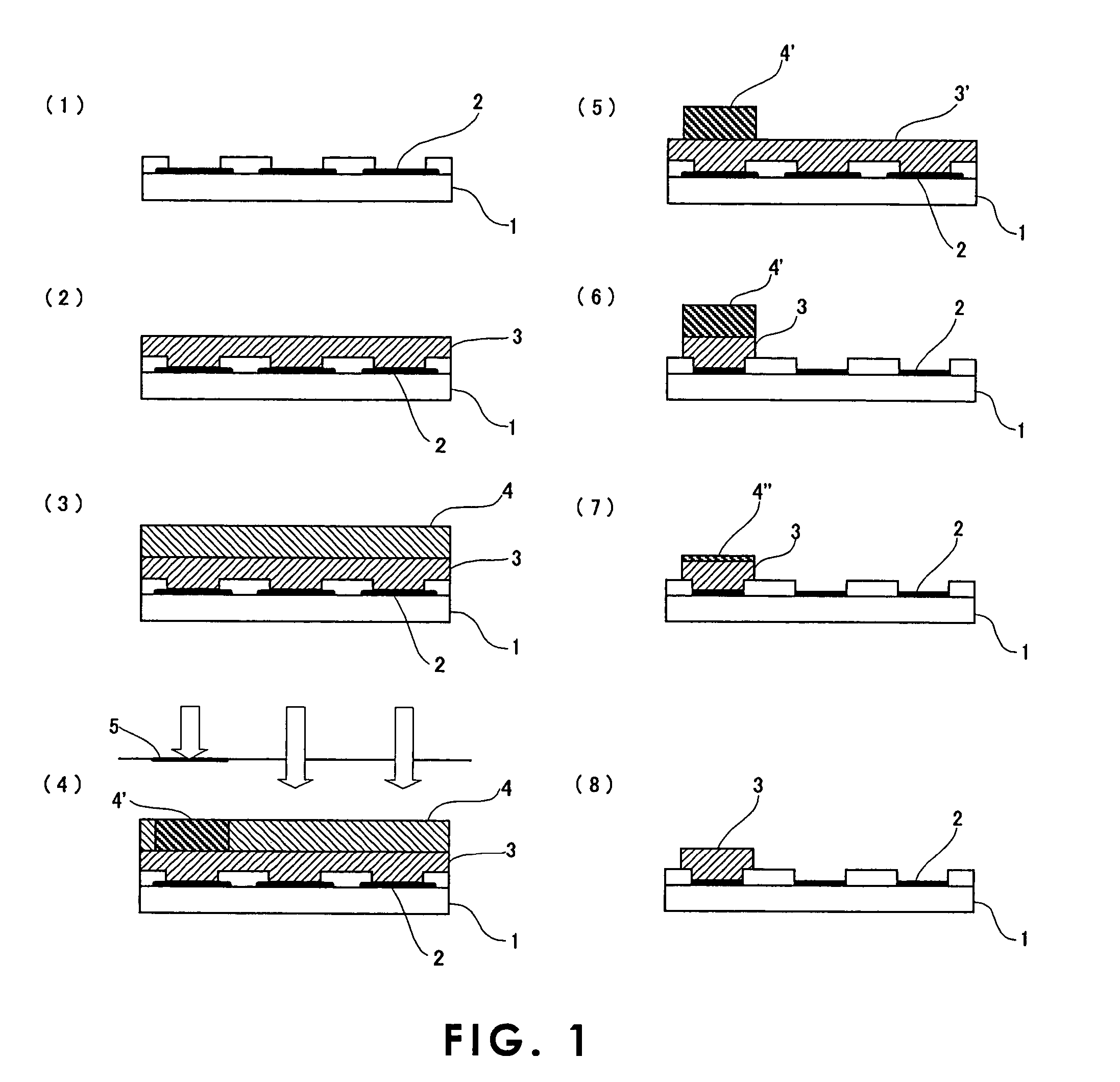
[0078](1) Provision of Base Material

[0079]Preparation of Coating Liquid for Buffer Layer Formation

[0080]γ-Glycidoxypropyltrimethoxysilane containing a glycidoxy group (—CHOCH2) as an organic functional group (TSL8350, manufactured by Toshiba Silicone Co., Ltd.) was added to a commercially available material for buffer layer formation (poly-3,4-ethylenedioxythiophene / polystyrene sulfonate: PEDT / PSS; Baytron P, manufactured by Bayer) to a concentration of 1% by weight based on the solid content of PEDT / PSS to prepare a coating liquid for buffer layer formation.

[0081]A substrate having a size of 6 in. square and a thickness of 1.1 mm with a patterned ITO electrode provided thereon was provided and was cleaned. The coating liquid (0.5 ml) for buffer layer formation prepared above was dropped on this substrate, followed by spin coating at 2500 rpm for 20 sec to form a buffer layer on the base material. The thickness of the buffer...

example 2

Removal of Surface Layer in Luminescent Layers by Plasma Treatment

[0097]An EL element 2 having a construction of base material / first electrode / buffer layer / luminescent layer (R, G, B) / second electrode was prepared in the same manner as in Example 1, except that, in the step of removing the surface layer part in the EL layers, the surface of the formed individual luminescent layers was subjected to plasma treatment. The plasma treatment was carried out in an argon gas atmosphere under conditions of RF power 200 W and chamber pressure 10 mTorr.

example 3

Removal of Surface Layer in Luminescent Layers with Solvent

[0098]An EL element 3 having a construction of base material / first electrode / buffer layer / luminescent layers (R, G, B) / second electrode was prepared in the same manner as in Example 1, except that, in the step of removing the surface layer part in the EL layers, a mixed solvent composed of monochlorobenzene and ethyl acetate (mixing ratio=1:1) was dropped on the surface of the formed individual luminescent layers, and the assembly was spun by spin coater at 3000 rpm to clean the surface layer part in the luminescent layers.


PUM

PropertyMeasurementUnit
depthaaaaaaaaaa
depthaaaaaaaaaa
thicknessaaaaaaaaaa

Abstract

There is provided a process for producing an EL element by photolithography, which process can produce an EL element having improved luminescence efficiency. The production process comprises the steps of removing a photoresist from photoresist layer-covered parts of an electroluminescent layer and cleaning the surface of the electroluminescent layer parts from which the photoresist has been removed.

Description

BACKGROUND OF THE INVENTION[0001]1. Field of the Invention[0002]The present invention relates to a process for producing an electroluminescent element. More particularly, the present invention relates to a process for producing an electroluminescent element, which can realize the provision of an electroluminescent element with high luminescence efficiency even by photolithography.[0003]2. Background Art[0004]Electroluminescent (hereinafter referred to as “EL”) elements have drawn attention as self-luminous planar display elements. In EL elements, holes and electrons injected from opposed electrodes are combined with each other within a luminescent layer, energy in this combination excites a fluorescent material within the luminescent layer, and luminescence of color depending upon the fluorescent material takes place.[0005]Among others, organic thin-film EL displays using organic materials as luminescent materials are very advantageous, for example, in that high-brightness luminesce...

Claims


Application Information

Patent Timeline
Patent Type & Authority Patents(United States)
IPC IPC(8): G03C5/00
CPCH01J9/2271G03F7/0007
Inventor TACHIKAWA, TOMOYUKIITOH, NORIHITOHASHIMOTO, KEISUKE
Owner DAI NIPPON PRINTING CO LTD
Why Eureka
Try Eureka