Organic light emitting diode display and method of manufacturing thereof

a light-emitting diode and organic technology, applied in the field of display technologies, can solve the problems of seriously affecting the luminescent properties of the oled, reducing etc., and achieves the effects of improving the luminescent characteristics enhancing the reflectivity of light, and greatly improving the luminous efficiency of the oled devi

Inactive Publication Date: 2020-06-18
WUHAN CHINA STAR OPTOELECTRONICS SEMICON DISPLAY TECH CO LTD
View PDF0 Cites 0 Cited by
  • Summary
  • Abstract
  • Description
  • Claims
  • Application Information

AI Technical Summary

Benefits of technology

[0046]The present invention forms a layer of reflective metal on the sidewall adjacent to the luminescent material of the pixel defining layer, so that the light emitted by the light emitting units is reflected to the display screen by the pixel defi

Problems solved by technology

When OLED emits light upward, a part of the light is obliquely passed through the pixel defining layer, whic

Method used


Image

  • Organic light emitting diode display and method of manufacturing thereof
  • Organic light emitting diode display and method of manufacturing thereof

Examples


Embodiment Construction

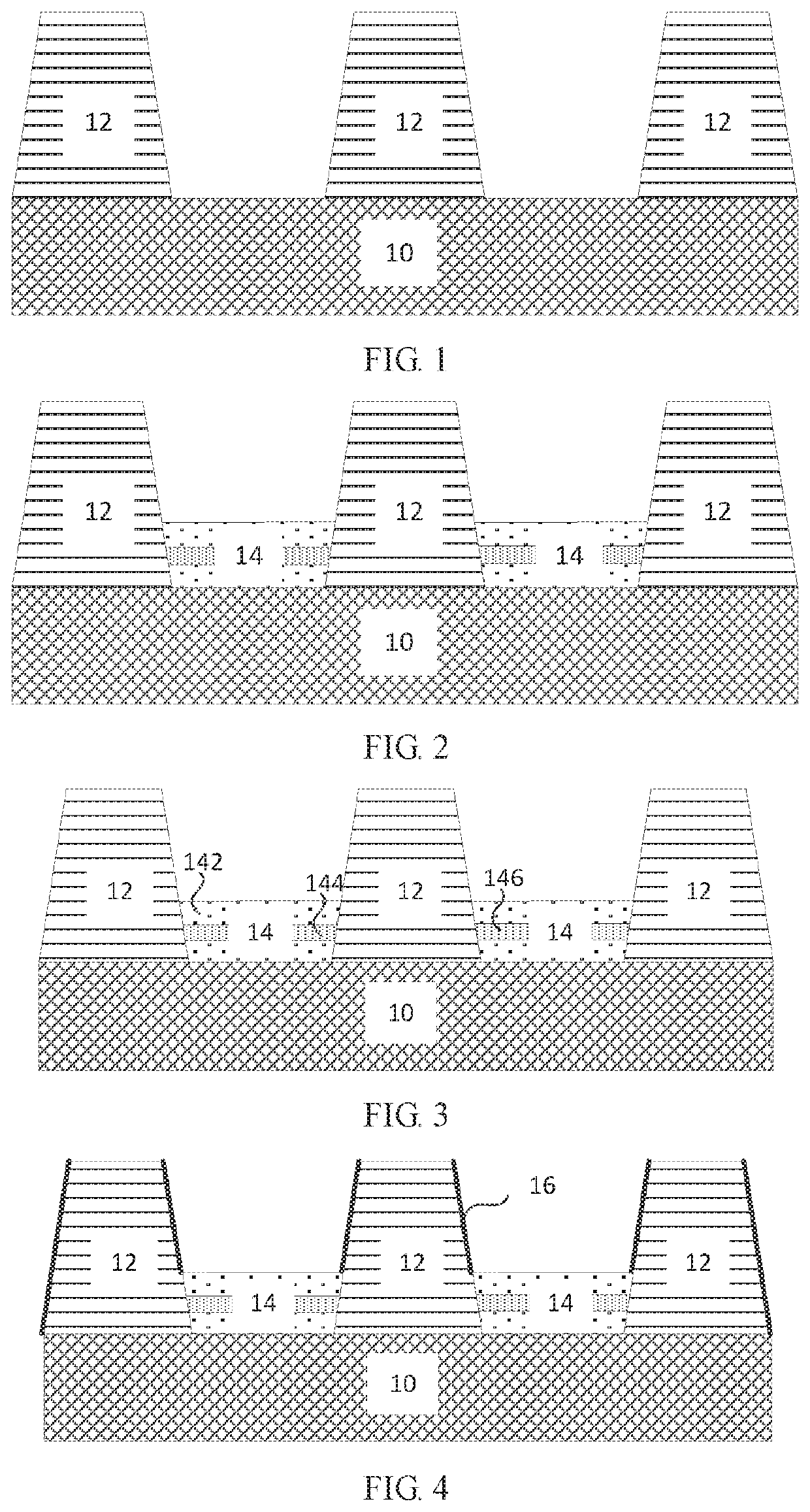
[0049]Description of following embodiment, with reference to accompanying drawings, is used to exemplify specific embodiments which may be carried out in the present disclosure. Directional terms mentioned in the present disclosure, such as “top”, “bottom”, “front”, “back”, “left”, “right”, “inside”, “outside”, “side”, etc., are only used with reference to orientation of the accompanying drawings. Therefore, the directional terms are intended to illustrate, but not to limit, the present disclosure. In the drawings, components having similar structures are denoted by same numerals.

[0050]The present invention provides an organic light emitting diode (OLED) display and a manufacturing method thereof, which solve the technical problem that light is absorbed by the pixel defining layer and affects the luminous efficiency of the OLED display. The present invention will now be described in detail with reference to the drawings.

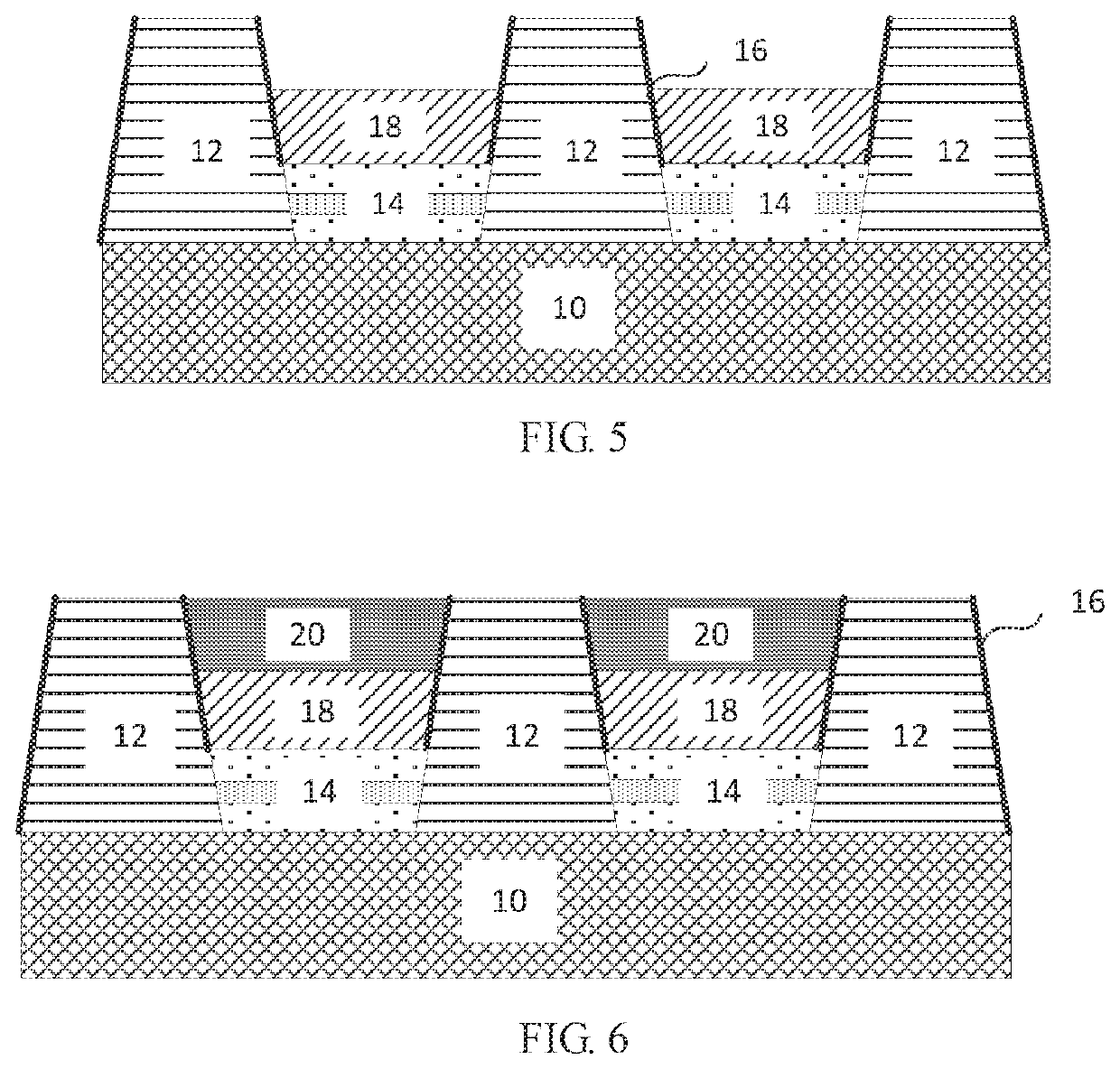
[0051]Referring to FIG. 6, FIG. 6 is a structural diagram of an...


PUM


Abstract

An organic light emitting diode (OLED) display and a method of manufacturing thereof are provided. The OLED display panel includes a substrate; a thin film transistor (TFT) layer on the substrate; a pixel defining layer above the TFT layer, the pixel defining layer having a via hole; a light emitting unit located in the via hole of the pixel defining layer, the light emitting unit includes an anode located at a bottom of the via hole, an organic light emitting material above the anode, a cathode located above the organic light emitting material, and a first reflective metal layer between the organic light emitting material and the pixel defining layer.

Description

BACKGROUND OF INVENTIONField of Invention[0001]The present invention relates to the field of display technologies, and in particular, to an organic light emitting diode (OLED) display and a method of manufacturing thereof.Description of Prior Art[0002]In a top emitting organic light emitting diode (OLED) display, each of the light emitting units includes an anode above a thin film transistor layer, an organic light emitting material above the anode, and a cathode over the light emitting material. Each adjacent light emitting unit is isolated from each other by an insulating layer, which is referred to as a pixel defining layer. The pixel defining layer is formed by depositing the insulating layer over the thin film transistor, and patterning the insulating layer by photolithography to form a plurality of through holes for manufacturing the light emitting units. In this way, each of the light emitting units is surrounded by an insulating material to achieve electrical insulation from...

Claims


Application Information

Patent Timeline
IPC IPC(8): H01L27/32
CPCH01L27/3262H01L27/3248H01L2227/323H01L27/3246H10K59/122H10K50/818H10K50/856H10K59/123H10K59/1213H10K59/1201
Inventor DING, WULI, SONGSHAN
Owner WUHAN CHINA STAR OPTOELECTRONICS SEMICON DISPLAY TECH CO LTD
Why Eureka
Try Eureka